The data acquisition technology involves a wide range of fields, and the dynamic range of the collected signals is wide, and the amount of processed data is large, which requires high real-time performance of the system. Processing signals in the form of digital signals has the advantages of fast processing speed, flexibility, accuracy, strong anti-interference ability, small size and high reliability, which meets the requirements for fast, accurate, real-time processing and control of signals. This design takes advantage of these advantages of digital circuits and improves on traditional analog recording circuits to improve performance at a lower cost.
1 Scheme Demonstration This design deals with audio signals in the form of digitized signals. There are three options to choose from:
1) Directly use the voice chip for voice recording and playback. Winbond's ISD series of voice chips use Chip-Corded patented technology, the sound can be stored directly without A/D conversion and compression, there is no A/D conversion error, and up to 250 levels of sound can be stored in one recording bit (BIT). The signal is equivalent to 8 times the recording capacity of the usual A/D technology. An on-chip crystal oscillator, mic preamp, automatic gain control, anti-aliasing filter, smoothing filter, sound power amplifier, etc., can form a complete sound recording and playback system with few peripheral components.
2) The DSP is used to process the sampled signal. DSP is a microprocessor with a special structure designed to quickly implement various signal processing algorithms. Its processing speed is far faster than that of a general CPU.
3) Using AT89S52 as the system main control chip, use ADC0809 to collect and A/D the audio signal, store the converted digital audio signal into the extended data memory, use the software to digitally filter the signal, and finally output through the single chip. The PWM signal is used to complete the playback.
From the economic and technical factors, the above three schemes are compared: direct use of the voice chip can reduce many peripheral circuits, and the circuit design is convenient, but the voice chip is not flexible enough. DSP has powerful digital signal processing functions and is flexible to use, but the chip is expensive and not suitable for general applications. The devices in scheme 3) are common chips, which are easy to obtain and the price is not high. Therefore, option 3) is the best design.
2 hardware design Figure 1 is the system hardware structure diagram. The audio signal converts the sound signal into a processable electrical signal through a pickup, and the preamplifier circuit is used to amplify the output of the pickup, and is matched with the A/D conversion circuit, and the A/D conversion circuit encodes the analog signal. The microprocessor is the core of the system. It is used to process and store digitized audio signals, coordinate the work of various parts of the system, and output PWM waves to drive the output circuits.
This article refers to the address: http://

2.1 MCU MCU is the control center of the system. It mainly realizes the following functions: controlling the LCD to display the relevant information of the voice signal, controlling the button recognition and function selection; controlling the collection of audio data and storing it in the Flash ROM, reading during playback The data in the Flash ROM uses the software method to generate the PWM pulse signal to realize the storage and playback of the voice.
2.2 Sound signal pickup and amplification circuit The sound signal pickup circuit is a device that converts a sound signal into an electrical signal. This design uses a microphone, which is an acoustic-sensitive resistor whose resistance changes with the change of the external sound signal. It is connected in series in the circuit, and the change of the resistance forms a voltage change. An electrical signal that characterizes the characteristics of the sound signal.
However, since the amplitude of the output voltage of the sound signal pickup circuit is small, 20 to 25 mV, if the signal is directly connected to the A/D conversion circuit, since the minimum resolution voltage of the A/D converter is also on the order of millivolts, it is generated. A large error, in order to ensure the accuracy of the system, before connecting with the A / D conversion circuit, an amplifier circuit must be connected in series, considering that the output signal of the sound signal pickup circuit is small, the distortion of the amplifier circuit and the accuracy of the noise to the system The most influential, so it is designed as a parallel negative feedback amplifier circuit with strong anti-common mode interference. Because the bandwidth of the audio signal is large, the dual-opput NE5532 with wide frequency band and low output impedance is selected.
2.3 A / D conversion circuit A / D conversion circuit consists of A / D converter ADC0809 and system processor AT89S52, mainly to achieve the sampling of the amplified sound signal. The circuit connection between ADC0809 and AT89S52 is shown in Figure 2.
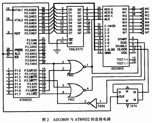
As can be seen in Figure 2, the ALE signal of ADC0809 is tied to the START signal, which causes the channel address to be written (latched) at the leading edge of the signal, followed by the conversion at the trailing edge. Only one P2.7=0 instruction is required to start A/D conversion. Prior to this, P2.7 is cleared and the address of the lowest 3 bits corresponding to the selected channel is sent to the data pointer DPTR. ADC0 809 conversion end signal EOC is reversed with AT89S52 ![]() Connected, read the A/D conversion result in interrupt mode, and start the next A/D conversion. It is also possible to start A/D conversion at regular intervals and read the last conversion result.
Connected, read the A/D conversion result in interrupt mode, and start the next A/D conversion. It is also possible to start A/D conversion at regular intervals and read the last conversion result.
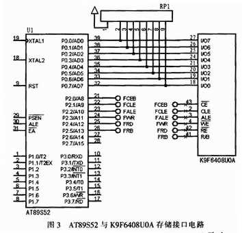
2.4 The sound code storage circuit generates a 1-byte digital coded signal at each sampling point during sampling. Since the sampling frequency is 8 kHz, if recording for 15 minutes, the required storage space is 7.031 25 MB. Therefore, the system uses 8 MB of flash memory K9F6408U0A, because the address line and data line of the memory can be reused, which can save I / O interface. The biggest advantage of the K9F6408UOA is that its command, data and address can communicate with the main controller through 8 I/O interface lines, which greatly simplifies the connection of the system and enhances the stability of the system. In addition to the eight I/O interface lines, the K9F6408 UOA also includes the following control lines: 1) CLE: Command Latch Enable, active high. in ![]() On the rising edge of the signal, the command signal can be locked into the command register through the I/O port; 2) ALE: The address latch enable terminal is active high. in
On the rising edge of the signal, the command signal can be locked into the command register through the I/O port; 2) ALE: The address latch enable terminal is active high. in ![]() On the rising edge of the signal, the address signal can be locked into the address register through the I/O port; 3)
On the rising edge of the signal, the address signal can be locked into the address register through the I/O port; 3) ![]() : Chip select line, active low. During a page or block erase operation or when the device is busy,
: Chip select line, active low. During a page or block erase operation or when the device is busy, ![]() High level will be ignored, 4)
High level will be ignored, 4) ![]() : Write enable port, command, address and data in
: Write enable port, command, address and data in ![]() The rising edge of the signal is locked; 5)
The rising edge of the signal is locked; 5) ![]() : Read the enable port, send data to the I/O port line on the falling edge of the port, and add 1 to the internal column address register; 6) WP: write protection port, active low, when it is low , program erase operation is prohibited; 7) R / B: operation status indication signal. When low, it indicates that a program is being programmed, erased or read, and becomes high after the operation ends. The above control line is utilized to facilitate the control of the K9F6 408U0A by the system main controller. AT89S52 microcontroller and K9F6408UOA storage interface circuit shown in Figure 3.
: Read the enable port, send data to the I/O port line on the falling edge of the port, and add 1 to the internal column address register; 6) WP: write protection port, active low, when it is low , program erase operation is prohibited; 7) R / B: operation status indication signal. When low, it indicates that a program is being programmed, erased or read, and becomes high after the operation ends. The above control line is utilized to facilitate the control of the K9F6 408U0A by the system main controller. AT89S52 microcontroller and K9F6408UOA storage interface circuit shown in Figure 3.
2.5 PWM output circuit This design uses the single-chip output PWM signal to drive the audio amplifier circuit. The PWM output circuit is shown in Figure 4. PWM is an effective technique for controlling analog circuits using digital output of a microprocessor. Modulation of the width of a series of pulses is equivalent to obtaining the desired waveform, and the system cost is much reduced because the D/A converter is not used. The advantage of PWM is that the signal from the processor to the controlled system is digital, no D/A conversion is required. Keeping the signal in digital form minimizes the effects of noise. In addition, the PWM signal is easily controlled by the MCU software, even if the circuit is slightly systematic, it is easy to correct by software.
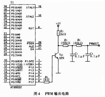
In Fig. 4, the PWM signal of a certain width is outputted by the P1.7 pin of the single-chip microcomputer, and after being shaped by the triode, it acts on the inertia link, and the obtained output signal PWMOUT will act on the audio power discharge path and be restored to sound.
2.6 Audio Power Amplifier Circuit In order to make the system have a large enough output, the speaker sound is driven to adjust the volume. After the PWM output circuit, the audio signal power amplifier LM386 is used to construct the power amplifier circuit, as shown in Figure 5.
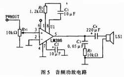
The LM386 audio power amplifier is mainly used in low voltage consumer products. To minimize peripheral components, the voltage gain is built into 20. However, by connecting resistors and capacitors between pins 1 and 8, the voltage gain can be adjusted to any value up to 200. The input is referenced by the status, and the output is automatically biased to half the supply voltage. At 6 V supply voltage, its static power consumption is only 24 mW, making the LM386 ideal for battery-powered applications. PWMOUT is the output of the PWM output circuit, and the speaker is 8 Ω, 0.5 W. After debugging, it is found that filtering the power supply +5 V with 10μF and 0.1μF capacitors will reduce a lot of noise and the effect is better.
3 system software design system has the functions of recording, playback, pause, clear storage content, various functions are selected by the button, the system first scans the status of each button, if there is a button press, it will transfer to the corresponding processing program, the system The program flow is shown in Figure 6.
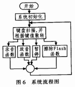
3.1 System Initialization Program The system initialization program mainly sets the individual variables to be used in the MCU interrupt, timer, LCD initialization, keyboard, PWM, K9F6408UOA storage interface, and ADC0809 address and program.
3.2 Key Scanning Program Since the recording and pause are set by two buttons connected to the external interrupt pin, once the button is pressed, the recording or playback program is entered, so the button scanning program is used to scan the playback button and the clear button. Whether to press.
3.3 The recording program is pressed with the button connected to the external interrupt O to enter the recording program.
The recording process is essentially the process of starting the ADC0809 to sample the analog audio signal and storing the A/D conversion result in the peripheral data memory. Therefore, it mainly includes reading the ADC0809 and writing the peripheral data memory into two parts. .
When extracting sound data, pay attention to the relationship between sampling frequency, number of sampling bits, storage capacity and storage time. Usually, the sampling frequency of 8 kHz and the number of sampling bits of 8 bits can obtain clear speech and better music sound, and occupy more Less storage space.
Start ADC0809 with a sampling frequency of 8 kHz, and read the last sampling result. The code fragment written to the external flash memory is as follows: 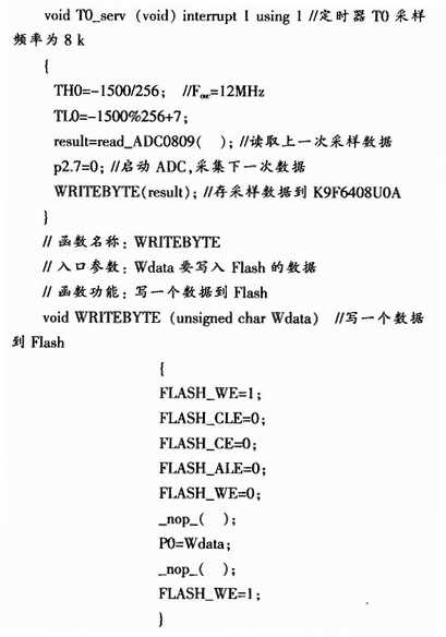
3.4 If the playback program is P1. O Press to execute the playback program. The playback process essentially reads the data in the peripheral data memory, converts it into a PWM wave of a certain width, and performs the output process. The subfunctions for reading K9F6408UOA are as follows: ![]()
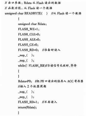
To generate a PWM waveform: 1) Set the timer to generate a timer interrupt. If the sample rate is 11.025 kHz, set the timer's timer interrupt frequency to 11.025 kHz. 2) Initialize the PWM module to generate 11.025 kHz. PWM waveform; 3) Wait for the timer interrupt, take the sample data in the interrupt handler, and set the PWM duty cycle register to determine whether the sound is played. If completed, the timer is turned off and the PWM output is stopped.
3.5 Suspending the program During recording, if you need to temporarily stop recording, you can press the Pause button to enter the pause state, and press the Pause button again to return to the previous state. A variable is set in the program to indicate whether it should be paused or resumed now.
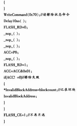
3.6 Memory Content Clearer When the memory content is full and you need to record, you can press the clear button to clear the content of a certain amount for the user to use again.
Erase: Erase in block units. The code fragment is as follows. 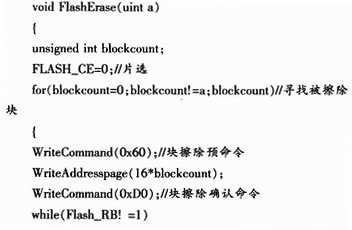
4 Debugging precautions When debugging the system, pay attention to the following aspects:
1) Since the sampling rate of 8 kHz is used in both the PCM (Pulse Code Modulation) encoding and the DPCM encoding mode, each compression interrupt service routine must be completed in less than 125 μs, so the compressed recording processing program The code must be optimized to minimize the execution time of the program to avoid conflicts between sampling and data processing or information display, and to avoid the loss of sample points when interrupting sampling.
2) When selecting the clock of ADC0809, the classic selection is about 640 kHz. The ALE terminal of the MCU is selected as the clock signal of ADC0809, but it is found that it affects the output display of the LCD. After changing ALE to 2 (triggered by 1 M) as the clock signal of ADC0809, the problem is solved.
3) Use the MAX813L reset chip instead of the RC reset circuit to reliably reset the circuit. The watchdog function is implemented in conjunction with software monitoring.
4) When the sampling frequency is 8 kHz and the word length is 8 bits, the storage language duration is longer than 15 min, and the playback voice quality is good.
5 Conclusion Using K9F6408UOA 8 MB NAND Flash memory and microcontroller PWM function can add voice function for the application of single chip microcomputer. The way the sound sampled data is stored is with direct, raw sampled data. In the specific practical application, the STC12C5A08AD with embedded A/D converter can be used, which can eliminate the external expansion ADC0809 and make the circuit more concise. The innovation lies in the fact that the dedicated voice chip is not used to realize the storage and playback of the voice of the single-chip application system.
Ningbo Autrends International Trade Co.,Ltd. , https://www.vapee-cigarettes.com