The X24128 is a CMOS serial communication EEPROM manufactured by XICor Corporation of the United States. The internal structure is a 16k byte 8-bit array. The X24182 can be connected in parallel at the same time on a 2-wire bus with software and hardware write protection. The highest on-chip address unit (FFFFH) is a write protect register. Three different forms of write protection are available for software write protection, block lock selection protection, and programming hardware write protection by writing different data. The highest clock frequency for serial communication on a 2-wire bus is 400 kHz. It also has input and output noise cancellation and suppression functions. Moreover, the power consumption is low, its read state operating current is less than 1 mA, the write state operating current is less than 3 mA, and the quiescent current is less than 1 uA. Operating voltages are available in 1.8V-3.6V, 2.5V-5.5V and 4.5V-5.5V versions. The writing method is in the form of byte writing and page writing, and each page is 32 bytes.
1. Pin descriptionThe X24128 is available in three package styles: 14-SOIC, 16-SOIC, and 8-PDIP. Figure 1 is an outline view of an 8-PDIP package. The function of each pin is described as follows:
VCC, Vss: the positive and negative input terminals of the power supply;
SCL: serial clock input for controlling the input and output of data;
SDA: Shared pin for serial data input and output. The drain output can be line or logically related to the output of the SDA pin of other devices. Since it is a drain output, it must be connected to a pull-up resistor during use;
WP: Hardware write protection input pin. When the WP pin is tied high and the WPEN bit of the write protection register is written to 1, the write-protected dummy register is write-protected, and the block-locked memory array can no longer be rewritten by the program. When no write protection is required, the WP pin is connected to a low level;
The S0, S1, and S2 devices select inputs. Up to eight X24128s can be connected in parallel on the serial communication bus, which can enjoy the bus in a time-sharing manner. In the input address, when the data of the first byte (device address) matches the input pins S0, S1, S2 of the device, the device is selected and can communicate serially with the CPU. If it does not match the input pin of the device, it is in a wait state.
2. Address selectionThe X24128 internal EEPROM consists of 16k & TImes; 8 bits, the address of this 16k data unit is 0000H-3FFFH. The address of the write protection register is FFFFH. Each address can be divided into an address high byte BYTE1 and an address low byte BYTE0. In addition to the data unit address, there is also a device address. In the device address, the upper four bits must be 1010, which is the identification code of the X24128. The three bits S2, S1, and S0 are the address codes of the selected devices, and they must match the input pins S2, S1, and S0 of the selected device. For example, if the S2 pin of the selected device is connected to Vcc, and the two input pins of S1 and S0 are connected to Vss, the device address should be 1010100R/WB. The bit is the read and write select bits. When the bit is 1, the read is selected. When the bit is 0, the write is selected.
3. Write protect registerThe write protect register is a readable register in the following format: the status of each bit can be written by the program. The function description is as follows:
WEL: Write enable latch for EEPROM array. When WEL=1, the write enable latch is set and can be written. When WEL=0, the write enable latch resets and rejects all write operations.
RWEL: Write enable latch for “write protection registerâ€. When RWEL=1, the “write protection register†can be rewritten. When RWEL=0, the write enable latch resets and rejects rewriting.
Both WEL and RWEL are reset at power-on.
BL1, BL0: EEPROM array block lock protection bits. The entire EEPROM array has three locking forms. When BL1 and BL0=00, the entire array is not block-locked. When BL1 and BL0=01, the array with the address 3000H to FFFH is block-locked. When BL1 and BL0=10, the address is Block lock protection for arrays of 2000~3FFF; when BL1, BL0=11, the array with address 0000H~3FFFH is block-locked.
WPEN: Write protection enable bit. When the WPEN bit is written to 1 and the WP pin of the device is connected to Vcc, the hardware write protection is enabled. When the WPEN bit is reset or the WP pin is connected to Vss, the hardware writes. Protection is no longer enabled. Hardware write protection can provide convenience for the entire system to implement write protection operations for users in actual application operations.
A memory array that is block-locked by the BL1 and BL0 bits is not affected by hardware write protection. The area of ​​the block-lock protection array can only be changed by changing the values ​​of BL1 and BL0. However, changing the values ​​of BL1 and BL0 is subject to the RWEL bit. The change in the RWEL bit is again constrained by hardware write protection. Arrays without block lock protection are not subject to hardware write protection and can be written to.
In the case of no hardware write protection, the rewriting of BL1 and BL0 can be performed in the following three steps:
1) Write 00000010 to the FFFFH address to make WEL=1;
2) Write 00000110B to the FFFFH address, so that RWEL=1;
3) Write X00XX010B to the FFFFH address so that RWEL=0. Register write protection. If RWEL = 1 is made in step (3), the overwriting of the register is invalid. The register remains in the state of step (2).
4. Read and write timingSet the start state before performing read and write operations. The method is to command the SCL bus to remain high and set a high-to-low transition on the SDA bus. At the end of the communication, an end state needs to be set, that is, the SCL bus is protected high, and a low level transition to the high level is set on the SDA bus. After the end state is set, the device leaves the communication state.
Changes in communication data on the SDA bus must be made while the SCL bus is in a low state. When the SCL bus is high, the data is on hold.
During communication, the device receiving the data sends a negative impulse response signal to the device transmitting the data each time it effectively receives 8-bit data. During the operation, the X24128 generates a negative pulse on the SDA bus each time it receives 8-bit data (including receiving 8-bit address data). The width of the pulse continues until the end of the ninth clock pulse signal. During the read operation, each time the CPU receives the 8-bit data sent by the X24128, a negative pulse is sent on the SDA bus to indicate that the read is valid, and then the X24128 can continue to transmit data. If the X24128 does not receive the response signal, it stops transmitting data until the end signal is received, and the communication ends.
4.1 Write timing by byte
When writing a byte of data to a unit of the X24128 internal storage array that has no lock protection part, first set the start state, and then send the device address and data address byte 1 and byte 0 in turn, X24128 receives each time. After an 8-bit address byte, the acknowledgment signal is sent using the ninth clock pulse. After receiving the third response signal, the CPU transmits 8-bit data and receives the response signal, and finally sets the end state. After receiving the end signal, the X24128 begins writing the received data to the internal write process of the EEPROM array. During the internal write process, no signal is reacted to any external input, and the SDA pin outputs a high-impedance state.
4.2 write timing by page
When the CPU writes data to X24128, it can be written by page. Each page includes 32 bytes. It is written as a page by the way of writing at the beginning, but the X24128 internal address pointer is automatically generated after each byte data is written. After adding 1 to continue writing data, there is no need to write the address again. After the highest address on this page is written, the address pointer automatically returns to the lowest address on this page. If the data continues to be written, the written data will be overwritten. Only after sending the X24128 end signal, the X24128 will stop receiving data and start. Perform an internal write process.
4.3 Read current address data
If you want to read the data of the unit currently pointed by the X24128 internal address pointer, you can receive the data of the current address sent by X24128 as long as it is sent to the X24128 start signal, the device address (bit is 1), and the response signal is received. After the reception is completed, the end signal is sent. After the X24128 sends the data, the address pointer is automatically incremented by one.
4.4 reading data from any address
The address of the data to be read is first sent to the X24128, making it the address pointed to by the current address pointer. The bit of the device address is written to 0, and the data is read by reading the current address data.
4.5 Continuous reading of data
Continuous reading of data is like reading any address data, setting the first address of the data to be continuously read as the current address. After receiving the data of the first byte, it is not the end signal but the response signal, X24128 receives Continue to send the second byte of data after the response signal. As long as the CPU sends a response signal after receiving one byte of data, the X24128 will continue to send the next byte of data. When the highest address of the entire storage array is sent, the address pointer will return to 0000H. unit. If the acknowledgment signal continues to be sent, the X24128 will continue to transmit data from the 0000H unit. The transmission is terminated only when the end signal is received.
5. Interface circuit and programming
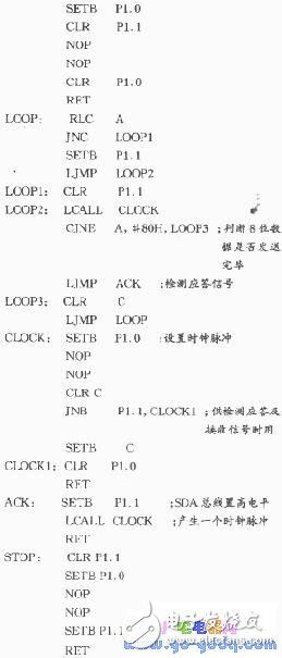
The interface circuit of X24128 and AT89C51 is shown as in Fig. 2. Up to 8 X24128s can be connected in parallel on the 2-wire bus. The P1.0 port line is used as the clock signal output, and the P1.1 port line is used as the data input and output. The bus is connected to a 4.7kΩ pull-up resistor. The following is an example of writing the data of the AT89C51 register R2 to the 1000H address of X24128(1). If the 1000H address is not write-protected, the programming is as follows:
·Basic precautions
Do not put expensive oil into low-quality cartridges to avoid wastage. Most pre-filled oil cartridges have the so-called 510 thread. The oil cartridge screws onto a rechargeable battery. Some of these batteries have buttons and some heat up automatically when you pump the oil. Some batteries have multiple temperature settings and some heat up to a preset temperature; these features need to be known in advance.
·Cleaning notes
Use a suitable cleaning tool to clean them, such as activated charcoal or dried tea leaves in a used pipe to absorb the oil. It is important not to use alcohol or other boiling water to clean the pipe, and to wait until it has cooled down completely before cleaning. Otherwise, the hot stem will come into contact with the watery liquid and cause the mouthpiece tenon to loosen, thus shortening the life of the 510 cartridges.
This is what you should be aware of when using 510 cartridges. At the same time, when using 510 cartridges, there are still some vaping tips, for example, when using them, be careful not to suck too hard, will not produce smoke. When you inhale too hard, the smoke is sucked directly into your mouth and not atomized by the atomizer, so gently inhaling is more powerful and gives you a better vaping experience.
510 Cartridge Oem,Leakproof 510 Cartridge,510 Battery And Cartridges Oem,510 Cartridge
Shenzhen MASON VAP Technology Co., Ltd. , https://www.disposablevapepenfactory.com