The circuit of the LED corridor light is shown below. The circuit is composed of a capacitor step-down circuit, a rectifier circuit, an LED lighting circuit, and a photoelectric control circuit.
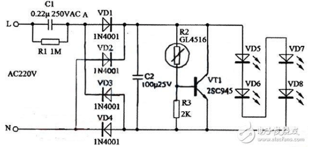
220V AC power through the capacitor C1, R1 step-down current limit after the AC voltage at A and B points is about 15V, rectified by VD1 ~ VD4. Get DC voltage of about 14V on C2 as high-brightness LED VD5 ~ VD8 The working voltage of the LED is about 14mA. Since the capacitor C1 does not consume active power, the power consumed by the bleeder resistor is negligible, so the power consumption of the entire circuit is about 15 & TImes; 0.014 ≈ 0-2 (W).
In order to further save power and extend the service life of high-brightness LEDs, a photoelectric control circuit consisting of a photoresistor R2, a resistor R3 and a triode VT1 is added to the circuit. At night, the resistance of the photoresistor R2 can reach 100K or more. The voltage across C2 is divided by R2 and R3, and the DC bias voltage supplied to the base of VT1 is very small. VT1 is cut off, which has no effect on the operation of the LED. During the daytime, due to the effect of photoelectric effect, the resistance of R2 can be Reduce to below 1OK, then VT1 is turned on and close to saturation. Since the current through C1 can only reach 15mA at maximum, the voltage on C2 can drop below 4V due to the shunt of VTl.
Led lamp drive power supply circuit diagram (2) LED drive power supply specific requirementsLED is a low-voltage light-emitting device with long life, high light efficiency, safety and environmental protection, and convenient use. For mains AC input power drives, the isolated output is based on safety specifications. The higher the efficiency of the LED driving power supply, the better the LED's high luminous efficiency and energy saving. At the same time, the high switching operating frequency and high efficiency make the entire LED driving power supply easy to install in compact LED lamps. High constant current accuracy guarantees brightness and color consistency when using LED lighting in large quantities.
Power LED lamp cup application scheme below 10WAt present, power LEDs below 10W are widely used, and many integrated products are available, that is, LED driving power and LED lights are integrated in one lamp, which is convenient for users to use directly. Typical lamp specifications are GU10, E27, PAR30 and so on. For this application, we have designed the following scheme (see Figure 1)
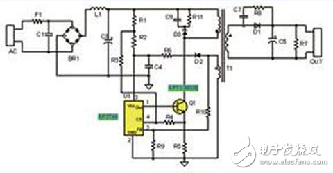
Figure 1: Schematic diagram of LED driver circuit based on AP3766
The program features are as follows:
1. Based on the latest LED dedicated driver chip AP3766, the primary side control mode is adopted, and the optocoupler and the secondary current control circuit are not needed to realize the isolated constant current output, and the circuit structure is simple. The primary side current is detected by the resistor R5, the primary current peak is controlled to be constant, and the switching duty ratio is controlled, and the on-time of the output diode D1 and the entire switching cycle time ratio are kept constant, and the output current is constant.
2. The AP3766 uses a proprietary “sub-micron startup current†technology that requires only 0.6μA of startup current, thus reducing power dissipation on the startup resistors R1 and R2 and improving system efficiency. Typical 5W application efficiency is greater than 80%, and no-load power consumption is less than 30mW.
3. AP3766 uses constant current tightening technology to achieve vertical constant current characteristics, high constant current accuracy.
4. The number of circuit components is small. The AP3766 is packaged in SOT-23-5, which is small in size. The whole circuit can be installed in the common specification lamp cup.
5. Safe and reliable, isolated output, with output open circuit protection, over voltage protection and short circuit protection.
6. The power switch tube adopts a triode, which eliminates the high-voltage field effect tube and has low system cost.
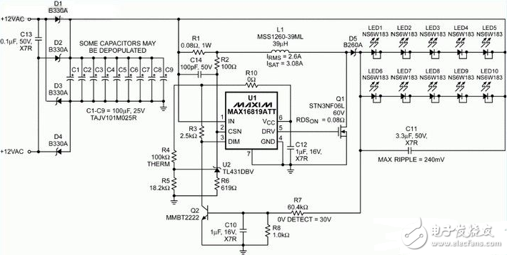
Led lamp drive power circuit diagram (3)Share a schematic of the driver circuit for an AR111 LED with a 2 and 5 string (5S2P) combination. The MAX16819 operates in buck-boost mode and operates at 12VAC to provide an average of 500mA of drive current per string of LEDs. This circuit uses MAX16819 as the main controller, which can drive a total of 10 LED-2 series and parallel, 5 LEDs per string. The input voltage is 12VAC and the tolerance is ±10%. Schottky diodes D1 to D4 form a full-wave rectifier circuit. Capacitors C1 through C8 are used for voltage filtering. According to the requirements of LED flashing, some filter capacitors can be removed to reduce the cost. These capacitors contain a tantalum capacitor with good temperature characteristics.
Since the LEDs are arranged in 5S2P, it is impossible to achieve a perfectly matched current. Assume that the LED lights have a good match to minimize current differences. Controlling the number of LEDs per string and the number of lamps in the hybrid architecture helps to mitigate the effects of current matching. As shown below.
This design uses TNY279 power chip as the control chip of Switching Power Supply. TNY279 power chip integrates a 700V high voltage MOSFET switch and a power controller on one device. Unlike ordinary PWM controller, it uses simple on/off control mode. To stabilize the output voltage. The controller includes an oscillator, an enable circuit, a current limit state regulator, a 5.8V regulator, an undervoltage or overvoltage circuit, a current limit selection circuit, overtemperature protection, current limit protection, and leading edge blanking circuitry. The chip features automatic restart, automatic adjustment of switching cycle turn-on time and frequency jitter.
Analysis of the working principle of the circuitThe core part of the power supply uses a flyback converter, which is simple in structure and easy to implement. The overall design circuit diagram is shown in Figure 1.
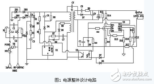
Considering the cost, volume and other factors, the improved harmonics adopt passive power factor correction circuit, which is mainly realized by improving the conduction angle of the input rectifying and filtering capacitor. The specific method is to connect the inductance between the AC input terminal and the rectifier bridge. As shown in Figure 1, C1, C2, L1, and L2 form a π-type electromagnetic interference filter, and fill the circuit with a valley filling circuit to reduce the total harmonic. Wave distortion. The valley filling circuit consists of D1, D2, D3, C3, C4, and R3, limiting the 3rd harmonic and 5th harmonic of the 50Hz AC current.
The rectified and filtered DC input voltage is applied to the primary winding of T1. The MOSFET integrated in U1 (TNY279) drives the other side of the transformer primary. Diodes D4, C5, and R6 form a clamp circuit that controls the drain leakage sense voltage spike of the drain to within safe limits. The combination of Zener diode clamping and parallel RC optimizes EMI and is more efficient.
High frequency transformer designThe TNY279 is fully self-powered, but with bias windings, output overvoltage protection can be used to protect the load in the event of an open-loop fault in feedback, effectively reducing the damage to the LED source. Bias windings are used in this design. As shown in Figure 1, the chip can be powered by a lower bias voltage, which suppresses the internal high-voltage current source and reduces the power consumption to less than 40MW at no load. Y capacitors reduce electromagnetic interference.
Feedback circuit designThe secondary uses constant current and constant voltage double loop control. The NCS1002 is a constant current and constant voltage secondary controller. As shown in Figure 2, it integrates a 2.5V reference and two high-precision op amps.
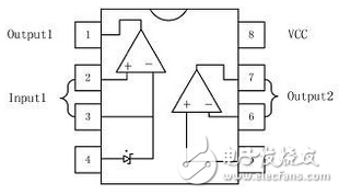
Figure 2 NCS1002 chip internal structure
The voltage reference and op amp 1 are the core of the voltage control loop. The op amp 2 is an independent op amp for current control. In this design, the voltage control loop is used to ensure the stability of the output voltage, and the current feedback control loop detects the average LED current, that is, the current on R17 in the circuit, converts it into a voltage and 2.5V reference comparison, and provides error feedback. Go to TNY279 to adjust the conduction.
working principle:The NCS1002 regulates the output voltage value. When the output voltage exceeds the set voltage value, current flows to the optocoupler LED, thereby pulling down the current of the transistor in the optocoupler. When the current exceeds the threshold current of the enable pin of TNY279, the next cycle will be suppressed. When the falling voltage is less than the feedback threshold, a switching cycle will be enabled. By adjusting the number of enable cycles, the output voltage is adjusted. Similarly, when the current on R16 is detected, that is, the output current is greater than the set value, the current is pulled through the other diode to pull down the current of the transistor in the optocoupler LED to achieve the purpose of suppressing the next cycle of TNY279, when the output current is less than the set value. The current will enable a switching cycle. Through such a feedback adjustment mechanism, the output voltage and current can be stabilized.
When the feedback circuit fails, that is, in an open-loop fault, when the bias voltage exceeds D9 and the bypass/multi-function pin voltage, current flows to the BP/M pin. When this current exceeds ISD (off current), the internal latch shutdown circuit of TNY279 will be activated to protect the load. Since the bias winding is used to feed current to the BP/M pin, the internal high voltage current source is suppressed. This connection reduces the no-load power consumption at 265VAC input to 40MW to reduce power consumption.
Led drive power is a power converter that converts the power supply to a specific voltage and current to drive led light. Usually, the input of the led drive power includes high-voltage power frequency AC (ie, mains), low-voltage DC, high-voltage DC, low-voltage high-frequency. AC (such as the output of an electronic transformer).

In the current LED power driver, electrolytic capacitors must be used, and small electrolytic capacitors can only last for several thousand hours. However, the use of the patented IC driver does not require the use of electrolytic capacitors, the life expectancy of more than 40,000 hours, 10 times that of the original driver, and the patented IC driver is small in size, only a quarter of the original area, can be easily put into In the LED bulb, it is not necessary to change the shape of the original bulb, so that the design is more simple and more acceptable to the user.
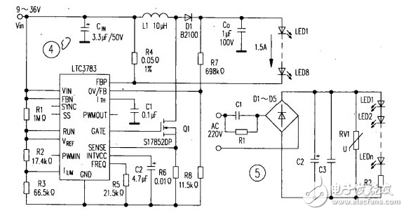
Led lamp drive power circuit diagram (six)A buck/boost converter must be used when the input voltage can be higher or lower than the total voltage drop of the LED or LED string. A circuit based on the LT°C3783 buck/boost converter drives eight 1.5A series LEDs as shown in Figure 4. The input voltage range of the LED string driving circuit is 9~36V, and the total voltage drop range of the LED string is 18~37V. Under the condition of VIN=14.4V, Vo=36V and I0=1.5A, the output power is 54W, and the efficiency is up to 93%. The switching frequency of the circuit is determined by the IC pin FREQ
Resistor R5 is set (frequency range is 20kHz~1MHz). The voltage divider composed of R7 and R8 sets the output overvoltage protection level. R4 is connected between IC pin FBP and high side line to sense LED current. The LTC3783 supports multiple topologies. It can also be used to construct circuits such as boost converters and buck converters.
Flyback converters, single-ended primary inductor converters (SEPIC), and CUK regulators can all increase or decrease the input voltage.
The output and input voltage can be the same or opposite in polarity. Each topology has unique advantages, but is less efficient than a buck-boost regulator.
Switching Power Supply
LED power supply, CCTV center power supply device, LCD display power supply.
We can meet your specific requirement of the products, like label design. The plug type is US/UK/AU/EU. The material of this product is PC+ABS. All condition of our product is 100% brand new. OEM and ODM are available in our company, and you deserve the best service. You can send more details of this product, so that we can offer best service to you!
Power Supply,5V Power Supply,12V Power Supply, 24V Power Supply
Shenzhen Waweis Technology Co., Ltd. , https://www.szwaweischarger.com