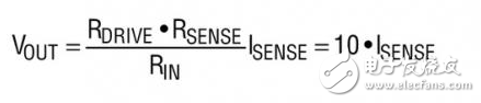
High-end current detection method based on power supply voltage of precision ultra-low power amplifier
The precision high-end measurement of the microamplifier current requires a small value sense resistor and a low offset voltage, ultra low power amplifier. A 280μA supply current is provided to sense current over a wide dynamic range of 100μA to 250mA. This minimizes the power loss on the shunt resistor and maximizes the available power of the load. The rail-to-rail input of the LTC2063 allows the circuit to operate at very small load currents with the input common mode almost in orbit. The LTC2063's integrated EMI filter protects it from RF interference under noisy conditions. For a given sense current, the voltage output of the circuit is:
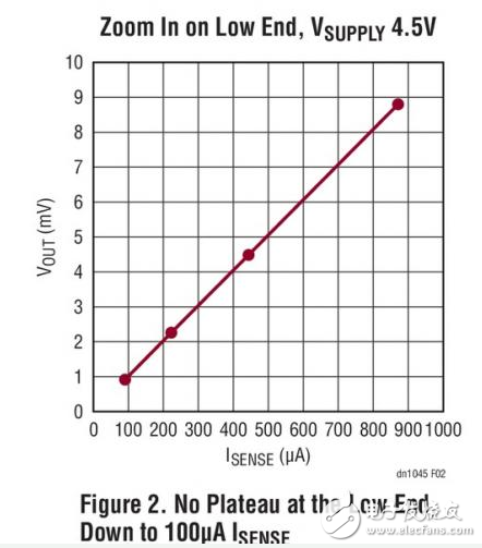
A key indicator of a current sensing solution is the zero point, or the equivalent error current of the output that is produced when no current is detected. The zero point is usually determined by the amplifier's input offset voltage divided by RSENSE. The LTC2063's low input offset voltage (1μV typical, 5μV maximum, typical input bias and offset current of 1-3pA) allows the zero input reference error current to be only 10μA (1μV/0.1Ω), typical It is 50μA (5μV/0.1Ω) maximum. As shown in Figure 2, this low error allows the detection circuit to maintain its linearity at the lowest current (100μA) within the specified range without the loss of resolution due to the loss of resolution. The output current to output voltage curve is throughout the entire current sensing range.
Another source of zero error is the zero gate voltage drain current (IDSS) of the output PMOS, which is the parasitic current of a non-zero VDS when the PMOS is nominally turned off (| VGS | = 0). A MOSFET with a high IDSS leakage will produce a non-zero positive VOUT without ISENSE.
The upper limit IDSS of Infineon's BSP322P transistor used in this design is 1μA at | VDS | = 100V. As a good estimate of the typical IDSS of the BSP322P, at room temperature, with VDS = -7.6V, the IDSS is only 0.2nA, the error output is only 1μV, or an equivalent 100nA input current error.
When measuring 0A input current.
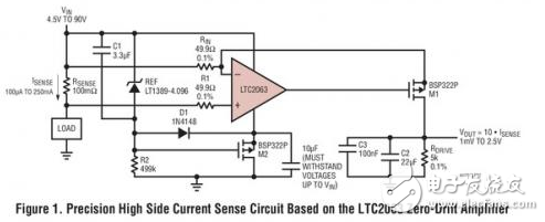
buildingThe LT1389-4.096 reference and the bootstrap circuit consisting of M2, R2 and D1 create a very low power, isolated 3V rail (4.096V + M2 VTH, typically -1V) that protects the LTC2063 from absolute The maximum supply voltage is 5.5V. Although the series resistor can meet the need to establish a bias current, the use of transistor M2 can provide a higher overall supply voltage while limiting the current consumption to only 280μA at the high end of the supply voltage.
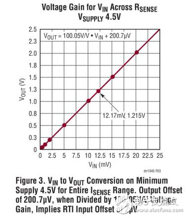
AccuracyThe LTC2063's input offset voltage produces a fixed input reference current error of 10μA. In the 250mA full-scale input, the offset only results in an error of 0.004%. At the low end, the error of 10 μA in 100 μA is 10%. Since the offset is constant, it can be calibrated. Figure 3 shows that the total offset of the LTC2063, mismatched parasitic thermocouple and any parasitic series input resistance is only 2μV.
The gain shown in Figure 3 is 100.05 V / V greater than the actual value given by RDRIVE and RIN or the expected gain given by 4.978k / 50.4 = 98.77V / V is 1.28. This error may be due to the different temperature coefficients of RDRIVE and RIN.
The main source of uncertainty in the output of this circuit is noise, so filtering with large parallel capacitors is critical to reducing noise bandwidth and total noise. With a 1.5 Hz output filter, the LTC2063 adds noise caused by a low frequency input of approximately 2μVP-P. The average output further reduces errors due to noise during the longest possible time.
Other sources of error in this current-sense circuit are the parasitic board resistance in series with the RSENSE input at RENS2063, the gain setting resistors RIN and RDRIVE's resistor value tolerance, the gain setting resistor in the temperature coefficient mismatch, and the error voltage in the parasitic thermocouple op amp enter. The first three sources of error can be minimized by using Kelvin sense 4 pin sense resistors for RSENSE and 0.1% resistors and similar or lower temperature coefficients for the critical gain setting paths of RIN and RDRIVE. To offset the parasitic thermocouple at the input of the op amp, R1 should have the same metal terminal as RIN. Asymmetrical thermal gradients should also be avoided at the input as much as possible.
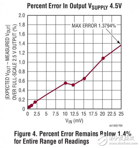
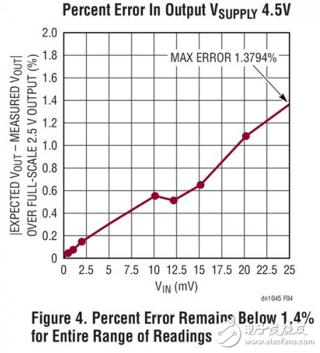
The overall contribution of all error sources discussed in this section is up to 1.4% at full-scale 2.5V output reference, as shown in Figure 4.
Supply currentAs shown in Figure 5, the minimum supply current required for the LT1389 and LTC2063 is 2.3μA at minimum VSUPPLY and ISENSE (4.5V and 100μA) and 280μA at maximum VSUPPLY and ISENSE (90V and 250mA). In addition to the current consumed by the active device, the output current IDRIVE to M1 provided by VSUPPLY is also required to be proportional to the output voltage, ranging from 1.0mV output (200μA for 100μAISENSE) to 500μA for 2.5V output (for 250mA ISENSE) . Therefore, in addition to ISENSE, the total supply current range is from 2.5μA to 780μA. Set RDRIVE to 5kΩ for a reasonable ADC drive value.
Input voltage range
In this architecture, the maximum supply is borne by the maximum | VDS | set PMOS output. The BSP322P is rated at 100V, so 90V is a suitable operating limit.
Output range
This design can drive a 5kΩ load, which makes it a suitable stage to drive many ADCs. The output voltage ranges from 0V to 2.5V. Since the LTC2063 has a rail-to-rail output, the maximum gate drive is only limited by the headroom of the LTC2063. In this design, the typical value is 3V, which is determined by the 4.096V of the LT1389 and the typical VTH of -1V of M2.
Since the output of this circuit is current, not voltage, ground or wire offset does not affect accuracy. Therefore, a longer lead can be used between the output PMOS M1 and RDRIVE, allowing the RSENSE to be near the sense current and RDRIVE close to the ADC and other subsequent signal chain stages. The disadvantage of long leads is the increased EMI sensitivity. The 100nF C3 on RDRIVE shunts harmful EMI before reaching the next stage of input.
Speed ​​limit
Since the LTC2063 has a gain-bandwidth product of 20 kHz, it is recommended to use this circuit to measure signals at 20 Hz or slower. The 22μFC2 in parallel with the load filters the output noise to 1.5Hz, which improves accuracy and protects subsequent phases from sudden current surges. This filtering compromise is a longer settling time, especially at the lowest end of the input current range.
in conclusionThe LTC2063's ultra-low input offset voltage, low IOFFSET and IBIAS, and rail-to-rail inputs provide accurate current measurements over the entire 100μA to 250mA range. Its maximum supply current is 2μA, making its circuit's supply current well below 280μA over most of its operating range. With the low supply voltage requirements of the LTC2063, low supply current allows power to be supplied from an alternate reference with a margin.
CBD tobacco oil can provide the same therapeutic effect as oral or sublingual CBD oil and tincture. Smoking this marijuana ingredient may help
you overcome nerves and stress; It can relieve pain, inflammation, insomnia, and other problems. CBD tobacco oil is a natural substance that
can be used to support and supplement your general health. Inhaling CBD is also one of the fastest ways to absorb this molecule and deliver
it to your blood, the ultimate destination.
cbd vape pen, cbd vape kit, cbd vape bar, cbd vape disposable,cbd vape devices
Ningbo Autrends International Trade Co.,Ltd. , https://www.ecigarettevapepods.com