
The single-chip RF device greatly facilitates the application of wireless communication in a certain range, and a complete wireless communication link can be constructed by using a suitable microcontroller and antenna combined with the transceiver. They can be integrated on a small circuit board for wireless digital audio, digital video data transmission systems, wireless remote and telemetry systems, wireless data acquisition systems, wireless networks and wireless security systems.
1. Potential contradiction between digital circuits and analog circuits
If the analog circuit (RF) and the digital circuit (microcontroller) work separately, they may work well, but once they are placed on the same board and work together with the same power supply, the whole system is likely to be unstable. . This is mainly due to the fact that digital signals oscillate frequently between ground and positive power supplies (3 V in size), and the period is extremely short, often ns. Due to the large amplitude and the small switching time, these digital signals contain a large number of high frequency components independent of the switching frequency. In the analog part, the signal transmitted from the antenna tuning loop to the receiving portion of the wireless device is typically less than 1 μV. Therefore, the difference between the digital signal and the RF signal will reach 10-6 (120 dB). Obviously, if the digital signal and the RF signal are not well separated, the weak RF signal may be destroyed, and the performance of the wireless device may deteriorate or may not work at all.
2. Frequently asked questions about RF circuits and digital circuits on the same PCB
Insufficient isolation of sensitive lines and noisy signal lines is a common problem. As mentioned above, the digital signal has a high swing and contains a large number of high frequency harmonics. If the digital signal wiring on the PCB is adjacent to a sensitive analog signal, high frequency harmonics may couple in the past. The most sensitive node of an RF device is typically a loop-locked loop of a phase-locked loop (PLL), an external voltage-controlled oscillator (VCO) inductor, a crystal reference signal, and an antenna terminal. These parts of the circuit should be handled with extreme care.
(1) Power supply noise
Since the input/output signals have a swing of a few volts, digital circuits are generally acceptable for power supply noise (less than 50 mV). Analog circuits are quite sensitive to power supply noise, especially for glitch voltages and other high frequency harmonics. Therefore, power line routing on PCB boards containing RF (or other analog) circuits must be more careful than wiring on a common digital board, and automatic routing should be avoided. It should also be noted that the microcontroller (or other digital circuit) will suddenly draw most of the current for a short period of time within each internal clock cycle, since modern microcontrollers are designed in a CMOS process. Therefore, assuming that a microcontroller is operating at an internal clock frequency of 1 MHz, it will draw (pulse) current from the supply at this frequency, which would cause a voltage spike on the power line if proper power supply decoupling is not taken. If these voltage spurs reach the power supply pins of the RF portion of the circuit, serious operation can be caused, so the analog power supply line must be separated from the digital circuit area.
(2) Unreasonable ground wire
The RF board should always be routed with a ground plane connected to the negative side of the power supply, which can cause some strange behavior if not handled properly. This may be difficult for a digital circuit designer to understand because most digital circuit functions perform well even without a ground plane. In the RF band, even a short line will act like an inductor. Roughly calculated, the inductance per mm length is approximately 1 nH, and the inductive reactance of a 10 mm PCB line at 434 MHz is approximately 27 Ω. If the ground plane is not used, most of the ground will be longer and the circuit will not guarantee design features.
(3) Radiation of the antenna to other analog parts
This is often overlooked in circuits that contain RF and other parts. In addition to the RF section, there are usually other analog circuits on the board. For example, many microcontrollers have built-in analog-to-digital converters (ADCs) for measuring analog inputs as well as battery voltage or other parameters. If the antenna of the RF transmitter is located near this PCB (or just on this PCB), the high frequency signal that is sent may reach the analog input of the ADC. Don't forget that any circuit line can emit or receive RF signals like an antenna. If the ADC input is not handled properly, the RF signal may self-excite within the ESD diode of the ADC input, causing ADC bias.
3. The solution of RF circuit and digital circuit on the same PCB
Some general design and routing strategies in most RF applications are given below. However, it is more important to follow the wiring recommendations for RF devices in real-world applications.
(1) A reliable ground level
When designing a PCB with RF components, a reliable ground plane should always be used. The goal is to create an effective 0 V potential point in the circuit, making all devices easy to decouple. The 0 V terminal of the power supply should be connected directly to this ground plane. Due to the low impedance of the ground plane, no signal coupling will occur between the two nodes that have been decoupled. It is important that the amplitude of multiple signals on the board differ by 120 dB. On a surface-mounted PCB, all signal wiring is on the same side of the component mounting surface and the ground plane is on the reverse side. The ideal ground plane should cover the entire PCB (except under the antenna PCB). If more than two layers of PCB are used, the ground layer should be placed on the layer adjacent to the signal layer (such as the next layer of the component surface). Another good method is to fill the vacant portion of the signal wiring layer with a ground plane that must be connected to the main ground plane through a plurality of vias. It should be noted that since the presence of the grounding point causes a change in the inductance characteristics of the side, the selection of the inductance value and the arrangement of the inductance must be carefully considered.
(2) Shorten the connection distance to the ground layer
All connections to the ground plane must be as short as possible, and the ground vias should be placed at (or very close to) the pads of the component. Never allow two ground signals to share a ground via, which may cause crosstalk between the two pads due to the via connection impedance.
(3) RF decoupling
Decoupling capacitors should be placed as close as possible to the pins, and capacitor decoupling should be used at each pin that needs to be decoupled. Using high-quality ceramic capacitors, the dielectric type is preferably “NPOâ€, and “X7R†works well in most applications. The ideal choice of capacitance should be such that its series resonance is equal to the signal frequency. For example, at 434 MHz, the SMD-mounted 100 p F capacitor will work well. At this frequency, the capacitance of the capacitor is about 4 Ω, and the inductive reactance of the via is in the same range. The capacitors and vias in series form a notch filter for the signal frequency, enabling efficient decoupling. At 868 MHz, a 33 p F capacitor is an ideal choice. In addition to RF decoupling small value capacitors, a large value capacitor should also be placed on the power supply line to decouple the low frequency, and a 2. 2 μF ceramic or 10 μF tantalum capacitor can be selected.
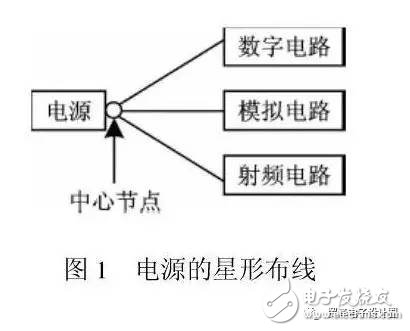
(4) Star wiring of the power supply
Star wiring is a well-known technique in analog circuit design (see Figure 1). Star Wiring—The modules on the board have their own power lines from a common power supply point. In this case, the star-shaped wiring means that the digital and RF sections of the circuit should have their own power supply lines, which should be decoupled close to the IC. This is a separation from the numbers
Partial and effective methods for power supply noise from the RF section. If a module with severe noise is placed on the same board, an inductor (bead) or a small value resistor (10 Ω) can be connected in series between the power line and the module, and a tantalum capacitor of at least 10 μF must be used for these. The power supply of the module is decoupled. Such modules are such as RS 232 drivers or switching power supply regulators.
(5) Reasonable arrangement of PCB layout
In order to reduce interference from the noise module and the surrounding analog portion, the layout of the various circuit modules on the board is important. Keep sensitive modules (RF sections and antennas) away from noise modules (microcontrollers and RS 232 drivers) to avoid interference.
(6) The effect of shielding RF signals on other analog parts
As mentioned above, the RF signal can cause interference to other sensitive analog circuit blocks such as the ADC when it is transmitted. Most problems occur in lower operating bands (such as 27 MHz) and high power output levels. It is a good design practice to use RF decoupling capacitors (100p F) to connect to ground to decouple sensitive points.
(7) Special considerations in the board loop antenna
The antenna can be made entirely on the PCB. Compared with the traditional whip antenna, it not only saves space and production cost, but also is more stable and reliable in the organization. Conventionally, a loop antenna design is applied to a relatively narrow bandwidth, which helps to suppress unwanted strong signals from interfering with the receiver. It should be noted that the loop antenna (as with all other antennas) may receive noise capacitively coupled by nearby noise signal lines. It can interfere with the receiver and can also affect the modulation of the transmitter. Therefore, do not place digital signal lines near the antenna, and it is recommended to keep free space around the antenna. Any object close to the antenna will form part of the tuning network, causing the antenna to tune away from the expected frequency, reducing the range of transmission and reception (distance). It must be noted for all types of antennas that the board's outer casing (peripheral package) may also affect antenna tuning. At the same time, care should be taken to remove the ground plane at the antenna area, otherwise the antenna will not work effectively.
(8) Board connection
If you connect the RF board to an external digital circuit with a cable, you should use a twisted pair cable. Each signal line must be twisted together with the GND line (DIN/GND, DOUT/ GND, CS/GND, PWR _ UP/ GND). Remember to connect the RF board and the digital application board with the GND cable of the twisted pair cable. The cable length should be as short as possible. The line that supplies the RF board must also be twisted with GND (VDD/ GND).
4 Conclusion
The rapidly growing RF integrated circuit provides the largest engineering and technical personnel engaged in wireless digital audio, video data transmission systems, wireless remote control, telemetry systems, wireless data acquisition systems, wireless networks and wireless security systems to solve the bottleneck of wireless applications. may. At the same time, the design of the RF circuit requires the designer to have certain practical experience and engineering design capabilities. This article is the experience that the author summed up in the actual development. I hope that many RF IC developers can shorten the development cycle, avoid unnecessary detours, and save manpower and financial resources.
Ningbo Autrends International Trade Co.,Ltd. , https://www.supervapebar.com