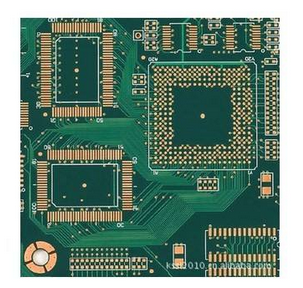
This paper analyzes the causes and causes of various interferences through several typical examples. It also introduces some special rules in the design of PCB (Printing Circuit Board) and the requirements of anti-jamming design.
With the rapid development of electronic technology, the density of PCBs is getting higher and higher, and the operating frequency of electronic systems is getting higher and higher; the use of analog circuits, digital circuits, large-scale integrated circuits and high-power circuits, and the work of electronic devices The bandwidth is wider and wider, and the sensitivity is higher and higher; along with the application of network technology, the cable and space networking between various devices is also becoming more and more complicated. Practice has proved that when we are using PROTEL software to make the board, despite the development of the relevant design rules and constraints. In the automatic layout and automatic wiring, improper design of the printed circuit board still occurs, and the reliability of the system is adversely affected. Therefore, in order to obtain the best performance of electronic systems, when using PROTEL software, the combination of automatic and manual must be adopted. And should follow the general and special rules of design.

Component wiring
1 . Minimize the wiring between high-frequency components and try to reduce their distribution parameters and electromagnetic interference between them. 2 . Some components or wires may have a higher potential difference between them, and the distance between them should be increased to avoid accidental short circuit caused by discharge. 3 . Electrolytic capacitors in the filter circuit, even though the connections are the same in the circuit diagram, have a wrong wiring order and do not provide the desired power ripple. 4. Consider the current loop. 5. General Configuration Principles of Capacitors 1) The input terminal of the power supply is connected with an electrolytic capacitor of 10μF to 100μF. If possible, better than 100μF. 2) In principle, a 0. 01pF ceramic capacitor should be arranged for each integrated circuit chip. If there is not enough space in the printed board, a 1pF to 10pF tantalum capacitor may be arranged for each (4 to 8) chips. 3) For devices with low noise immunity and large power supply changes during turn-off, such as RAM and ROM memory devices, decoupling capacitors should be directly connected between the power line and the ground of the chip. 4) Capacitor leads must not be too long, especially high-frequency bypass capacitors cannot have leads. 5) When there are contactors, relays, buttons and other components in the printed board, large spark discharges will occur when they are operated, and an RC circuit must be used to absorb the discharge current. Generally, R is 1kΩ to 2kΩ, and C is 2.2μF to 47μF. 6) The input impedance of CMOS is very high, and it is susceptible to induction. Therefore, when it is used, it should be grounded or connected to the power supply. 6. Oscillators Almost all electronic systems have an oscillator circuit coupled to an external crystal or ceramic resonator. Oscillation is a source of radiation.
General wire and pad routing
1. The minimum width of the printed board conductors is mainly determined by the adhesive strength of the conductors and the insulating substrate and the value of the current flowing through them. 2. Printed wire bends generally take arcs, and right angles or included angles can affect electrical performance in high frequency circuits. In addition, try to avoid the use of large area copper foil, otherwise, when heated for a long time, it is prone to the phenomenon of copper foil expansion and fall off. When a large area of ​​copper foil must be used, it is preferable to use a grid shape, which is advantageous to eliminate the volatile gas generated by the adhesive between the copper foil and the substrate. 3 . The center of the pad is also slightly larger than the diameter of the device lead.
Power line and ground design
1 . According to the size of the printed circuit board current, the width of the power line should be as thick as possible to reduce the loop resistance. At the same time, the direction of the power line and the ground line and the direction of data transmission should be the same, which helps to enhance the anti-noise ability.
2 . In a circuit where a small signal circuit is made with a large current circuit, GND must be clearly separated.
3 . Correctly select single-point grounding and multi-point grounding.
4 . Separated digitally from analog ground.
5. The grounding wire should be as thick as possible.
6 . The ground wire constitutes a closed loop.
Flat Control Cable Also known as festoon cable, this flat cable fits in confined spaces such as overhead cranes and hoists. It sends signal and data to operate, measure, or regulate automated equipment.
Raw cable can be UL2651, UL20251 ,etc
Flat cable, IDC cable, flat cable wiring, ribbon cable harness, flexible flat cable
ETOP WIREHARNESS LIMITED , https://www.wireharnessetop.com