First, evaluate design indicators
1. Input parameters: input voltage, AC or DC, phase, frequency, etc.
• The international voltage levels are single-phase 120Vac, 220Vac, 230Vac, etc. The internationally accepted AC voltage range is 85 to 265V. Generally include the input voltage rating and its range of variation;
• Single-phase input is often used for power below 3kW, and three-phase input is used above 5kW.
• Industrial power frequency is generally 50Hz or 60Hz, aerospace power supply, ship power consumption is 400Hz.
• With or without Power Factor and Total Harmonics Distortion indicators
2. Output parameters: output power, output voltage, output current, ripple, regulation (steady current) accuracy, adjustment rate, dynamic characteristics (settling time), start-up time and hold time of the power supply.
• Output voltage: rating + adjustment range. The upper limit of the output voltage should be as close to the rated value as possible to avoid unnecessary excessive design margin.
• Output current: rating + overload multiple. If there is a steady flow requirement, the adjustment range will also be specified. Some power supplies do not allow unloaded, so the lower current limit should also be specified.
• Regulated and steady current accuracy: Influencing factors include input voltage regulation, load regulation, and aging tolerance. The accuracy of the reference source, the accuracy of the detection components, and the accuracy of the op amp in the control circuit have a great influence on the stability of the voltage regulator.
3. Efficiency: Ratio of rated output voltage to rated output voltage, rated output current, and output active power.
loss:
The losses that are closely related to the switching frequency: the switching losses of the switching devices, the iron losses of the magnetic components, and the losses in the absorption circuit.
On-state losses in the circuit: On-state losses in switching devices, copper losses in magnetic components, and line losses. This part of the loss depends on the current.
Other losses: loss of control circuit, loss of drive circuit, etc. The efficiency of a power supply with a higher output voltage is generally higher than a power supply with a lower output voltage. High output voltage power efficiency can reach 90% to 95% efficiency. The efficiency of a high-power circuit can be made higher than that of a low-power circuit.
4. Voltage regulation and load regulation
• Voltage (source) adjustment rate: The power supply adjustment rate is usually the output voltage deviation rate caused by the input voltage change under rated load conditions. As the following formula shows:
Vo(max)-Vo(min) / Vo(normal)
Alternatively, the deviation of the output voltage must be within the specified upper and lower limits, that is, within the upper and lower absolute limits of the output voltage.
• Load Regulation: The load regulation ratio is defined as the ability of the switching power supply to provide a stable output voltage when the output load current changes. Or the output load current changes, the output voltage deviation must not exceed the upper and lower absolute value.
Test method: After the power supply of the tested power supply is stable under normal input voltage and load conditions, measure the output voltage value under normal load, and then measure the output voltage value under light load (Min) and heavy load (Max) respectively ( Vmax and Vmin), the load regulation ratio is usually a percentage of the output voltage deviation due to a change in the load current at a normal fixed input voltage, as shown by the following equation:
V0(max)-V0(min) / V0(normal)
5. Dynamic characteristics: the change of output voltage when the load suddenly changes
• The switching power supply ensures its output voltage is stable through the feedback control loop. In fact, the feedback control loop has a certain bandwidth, which limits the response of the power supply to changes in the load current and may cause the switching power supply to be unstable, out of control or oscillate. . In fact, the load current during power supply operation is also dynamically changing, so dynamic load testing is extremely important to the power supply.
• Programmable electronic load can be used to simulate the worst case load conditions of the power supply, such as rapid rise and fall of load current, cycle time, etc. If the power supply is under severe load conditions, it can maintain stable output. The voltage does not produce overshoot or undershoot. Otherwise, the output voltage of the power supply will exceed the load component (such as the TTL circuit, the instantaneous output voltage should be between 4.75V and 5.25V, which will not cause the TTL logic circuit. Misoperation) The scope of work.
6. Set-Up Time and Hold-Up Time
• Start-up time: refers to the time from when the power supply is connected to the power supply until the output voltage rises within the regulation range. Take a power supply with an output of 5V as an example. The start-up time is when the power supply is turned on and the output voltage reaches 4.75. V's time.
• Hold time: The time from when the power supply is turned off before the output voltage drops outside the regulation range. Take a power supply with an output of 5V as an example. The hold time is from shutdown until the output voltage is lower than 4.75V. The time is generally 10-20ms to avoid the impact of load operation due to short-term voltage interruption (half or one grid voltage cycle) in the power company's power supply.
7. Cross regulation of multiple output power:
• Multiple outputs also need to consider the Cross Regulation.
What is the cross adjustment rate?
The change range of the output voltage of the other circuit when the output load of one circuit changes.
The conventional method to improve the cross adjustment rate: rear adjustment
Such as: low-power multi-output Flyback
Input voltage range..............90~264VAC, 120-370VDC
Input current ..................2.0A/115V 1.1A/230V, input frequency: 47-63HZ
Inrush Current .................. Cold Start Current 20A/115V 40A/230V
Leakage current....................< 2mA/240VAC
Output voltage adjustment range ..........CH1 : -5 to +10%
Voltage regulation rate ................CH1:< 1%, CH2:< 1%
Load regulation ................CH1:<3% ,CH2/3:< 4-8%
Overload Protection ....................105%~150% Protection Type: Current Limit, Auto Recovery
Overvoltage Protection ..................115-135%CH1 Rated Output Voltage
Temperature coefficient: ±0.03%°C(0~50°C)
Start, rise, hold time... 800ms, 60ms, 20ms
Shock resistance .....................10 to 500Hz, 2G Triaxial 10min./1 cycle, 1 hour per axis
Pressure resistance .................... input-output: 3KVAC, input-case: 1.5KVAC,
Output - Housing: 0.5KVAC 1 minute
Insulation resistance...............Input-output, Input-ground, Output-ground 500VDC/100M Ohms
Operating temperature, humidity............-10C to +60C, 20% to 90% RH (0-45C/100%, -10C/80%, 60C/60 % LOAD)
Storage temperature, humidity............-20°C~+85°C, 10%~95RH
Dimensions ......................199*99*50mm CASE 916A
Weight......................0.6kg;20pcs/13kg/1.17CUFT
Safety Standards .................... Meets UL1310, TUV EN60950 Requirements
EMC/Harmonic Standards............... Meets EN55022 class B/A, EN61000-3-2, 3 EN61000-4-2, 3,4,5,6,8, 11, ENV50204
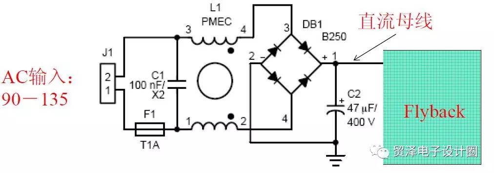
Second, select the appropriate main circuit topology (AC-DC)
Basic principles: power level, cost, efficiency, size
• Input harmonics are generally not limited when power is below 75 watts. Therefore, a flyback circuit with a simple circuit and low cost is selected. Japan limits 50W below. Higher lighting requirements, 25W.
• The general power supply requirements for circuit power above 75 W meet the harmonic IEC61000-3-2. Power factor correction is generally required, so two-stage solutions are mostly used.
Boost PFC+Flyback; <100W
Boost PFC+half bridge 100W<<500W
• Half-bridge or full-bridge can be used for higher power (above 500 watts). The cost is strict, half bridge is selected, and full bridge is selected for large power. Push-pull circuits are generally used in applications where the power is high and the input voltage is low.
• When the general power is less than 20W, the main circuit topology is simple because the loss of the power supply is dominated by magnetic components, switching, and drive loss, and the on-state loss is small (current is small). Such as DCM Flyback.
• When the power loss is dominated by on-state losses (high-power, or low-voltage, high-current), you need to consider a scheme that can reduce the on-state losses. For example: synchronous rectification, multi-level conversion, parallel connection, hybrid topology, etc.
Third, the design of components
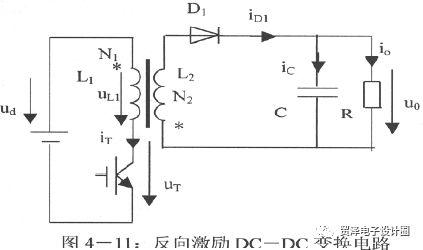
Example: Which components in the Flyback main circuit need us to design?

1 Calculate circuit operating parameters. Input and output voltage
2 operating parameters. Switching frequency, maximum duty cycle
3 Transformers.
4 Switch Tube - Voltage, Current
5 Secondary Diodes - Voltage, Current
6 output filter capacitor
7 absorption circuit
Design steps
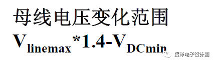
(A), determine the input DC bus voltage change range:
1) Range of change with input
2) Voltage change during each power frequency cycle
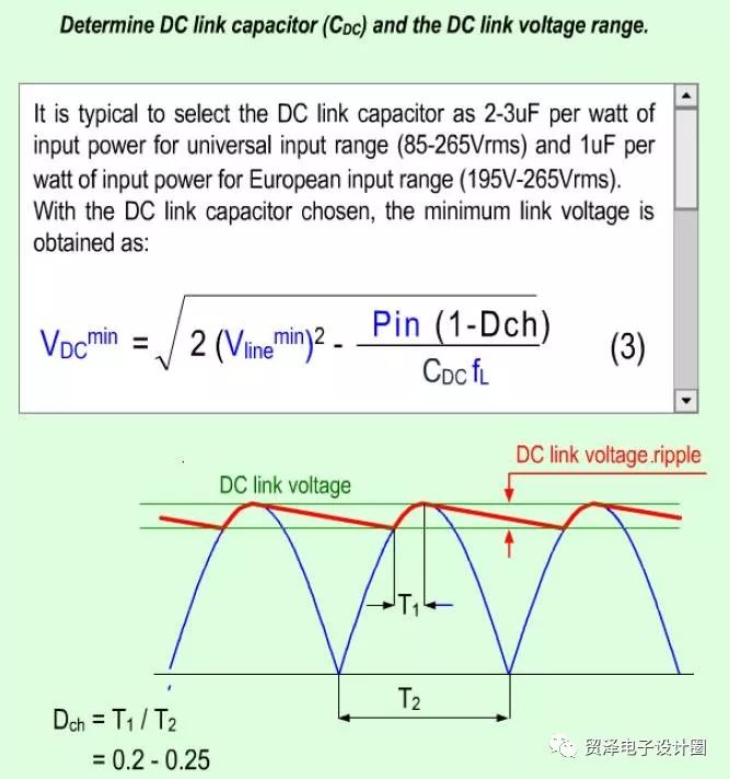
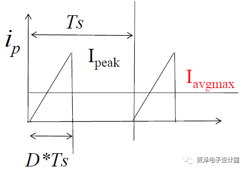
(B), design switching frequency fs, the maximum duty cycle Dmax = 0.45
• Set the switching frequency as required
• According to the input power, assuming the minimum voltage maximum duty cycle, just critical continuous, and then determine the peak inductor current
Pinmax=Pomax/efficiency
Iavgmax=Pinmax/VDCmin
Ipeak=2*Iavgmax/D
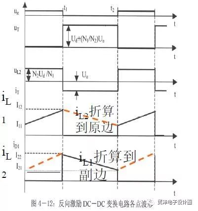
(III) Designing a flyback transformer
– Determine the primary inductance based on the maximum peak current
Pinmax=0.5*Lm*Ipeak2*fs
– Based on experience, select the core size and calculate the number of turns on the primary side.
Np=(Lm*Ipeak)/(Ae*Bmax)
Ae is the core cross-sectional area; Bmax is the design maximum flux density.
– Design air gaps based on inductance and number of turns.
– Select the appropriate turns ratio based on the rated voltage of the primary switch. In order to obtain better secondary cross regulation, it is sometimes necessary to adjust the number of turns of the transformer primary.
Example: Secondary Vo1: Vo2=5:3
A preliminary calculation results in: Ns1=3, Ns2=1.8; if Ns2 is taken as 2åŒ, the adjustment rate may be poor. Then, modify the number of secondary edges, Ns1=5 and Ns2=3.
(D), switch selection: power MOSFET
• Switch voltage stress:
Example: When the primary side selects a 650V MOSFET, the voltage stress of the primary switch should not exceed 600V.
Then calculate the maximum stress:
Vpmax=VDCmax+(Vo+Vdrop)*Np/Ns+60V
• Switch tube current stress:
– Calculate the maximum current of the primary side of the transformer
Under normal circumstances: Vo*N/Ns<140V;
Consider the stress of the primary switch, the voltage stress of the secondary diode, and the maximum duty cycle.
(E) Selection of secondary diodes:
– Fast recovery diode
– Calculate the withstand voltage of the diode
VD=(Vdcmax*Ns/Np+Vo)*1.3
(6) Output filter capacitor selection:
According to current/voltage stress, ripple requirements, choose electrolytic capacitors.
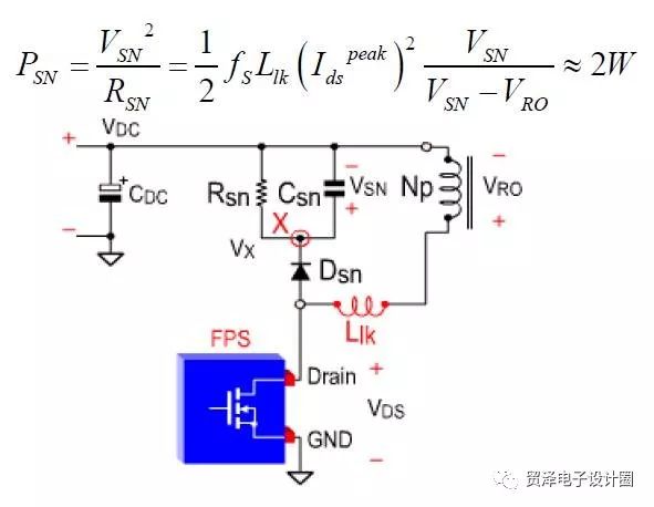
(seven), RCD absorption circuit
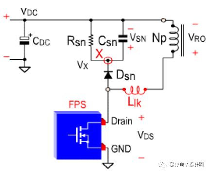
• Consider the issue:
1) Absorption effect
2) The loss is as small as possible
The trade-off between absorption and loss!
Not only for FLYback, but also for all existing R absorption circuits, the same design principles apply.
Loss estimation method:
1) Psnuber=Vc2/R
â—† When the MOSFET is turned off, when Vds exceeds the voltage VSN across the capacitor in the RCD snubber circuit, the snubber diode conducts. The spike current is absorbed by the RCD circuit, thereby reducing the peak current. The snubber capacitor must be large enough to guarantee a There is no significant change in the voltage across the capacitor during the switching period, but too large an absorption capacitance can increase the loss of the buffer circuit. Must be compromised.
â—† The power consumed by the absorption circuit can be calculated by the following equation. Take the resistance of 3W power resistor, the resistance and capacitance value can be calculated by software, as shown below
Guangzhou Yunge Tianhong Electronic Technology Co., Ltd , https://www.e-cigarettesfactory.com