This design takes PAF600F24-28 power module as the core, adopts the method of input parallel output and series connection to realize the voltage conversion of DC 24V to 75V. The external potentiometer can be used to adjust the output voltage within a certain range, and the output voltage can be adjusted within the range of -60% yoke + 10% of the nominal value. The output voltage of a single module can be adjusted up to 28VI 110%=30.8V, and the minimum output voltage can be adjusted to 28VI 60%=16.8V. When these three modules are used in series, a wide voltage output range can be obtained: 50.4V ray 92.4V. When the output of the three modules is adjusted to 25V, 75V is obtained. At this time, the output current is 600 clothes 25 = 24A. At the same time, the booster power supply also has a series of protection functions such as start control, voltage monitoring, overcurrent, overvoltage and overheating to ensure safe and reliable power supply operation. The three-module series working principle diagram is shown in Figure 1.
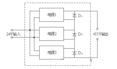
Figure 1 Module series boost schematic
Figure 2 shows the application circuit of a single power module. The input electrolytic capacitor C1 is a storage capacitor and can absorb the voltage spike at the input of the module. C2 and C3 are common mode filter capacitors, and 2kV high voltage ceramic capacitors are used. D1 is a transient absorption diode TVS, which protects against voltage transients and shocks. It prevents transient high-voltage spikes at the input of the power supply and damages the power module. The TVS also has an electrostatic protection function, which is of great significance for ensuring the safety of the module. . In addition, the use of the fuse can also prevent accidental reverse connection at the input end and damage the module.
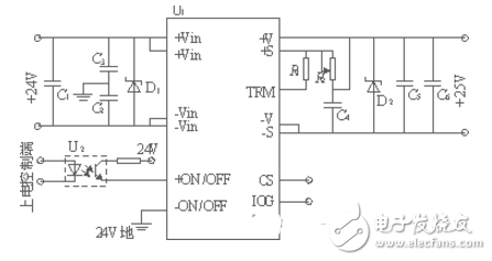
Figure 2 Application circuit of a single power module
Scheme comparisonFigure 3 is a block diagram of the boost power supply for the discrete component scheme. In this solution, each functional unit must be designed separately, and the overall design integration is low. Especially the isolation step-up transformer and H-bridge power conversion circuit, because it is not a special design, can only use conventional products, resulting in too large volume, and the entire design is not fully aging test and actual work verification, so often need to go through more Repeated revisions and improvements to meet design requirements are time consuming and labor intensive. In the DC/DC module, the power transformer and the H-type power bridge are designed in a flat special form, which is integrated into the module package, which saves space. And the power module technology is already very mature, and the reliability is extremely high. The designer only needs to use the module as the core to carry out certain peripheral design, rationally utilize the serial and parallel technology of the module, and realize the boost or power expansion according to the design requirements. A high-reliability integrated power supply that meets the requirements of technical specifications and works well. Compared with the discrete solution, the design cycle is shortened, and the reliability and technical indicators are greatly improved.
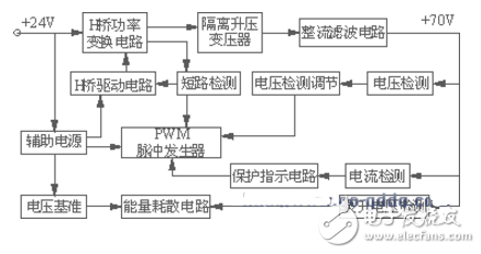
Figure 3 Block diagram of the booster power supply for the discrete component solution
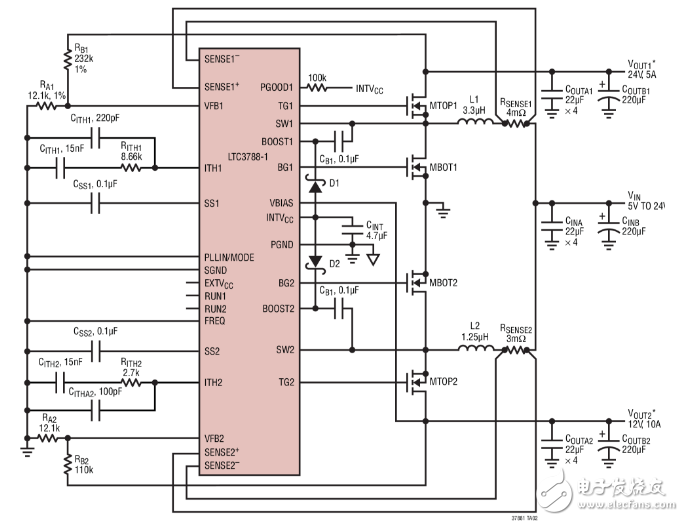
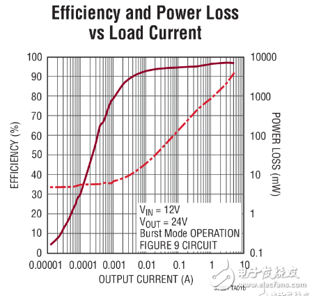
24v boost circuit diagram (2)The buck-boost converter shown in the figure can regulate a voltage of 24V and provide a load current of 0A to 5A with an efficiency of up to 98.5%. The device operates from an input voltage range of 12V to 58V. Adjustable undervoltage and overvoltage lockouts are used to protect the circuit. It has a short-circuit protection function and the SHORT output flag will signal when a short-circuit fault occurs on the output. The device performs DCM operation under light load conditions for lowest power consumption and reverse current protection. ROUT is responsible for limiting the output current during short-circuit and overload conditions, making it a robust application circuit.
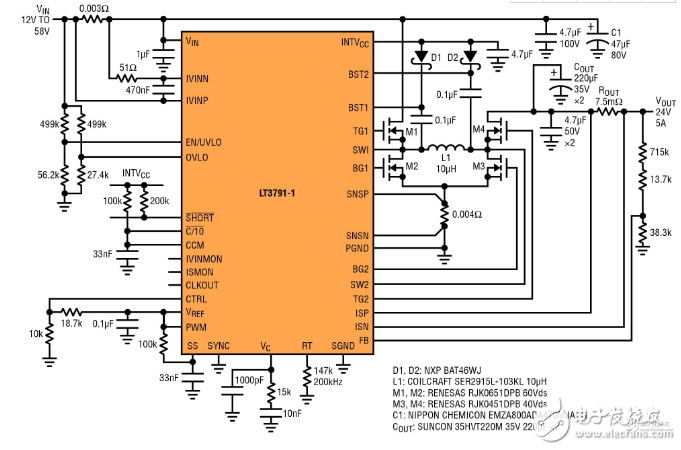
The LTC3788-1 is a high performance, two-phase, dual-channel, synchronous boost converter controller for driving full N-channel power MOSFETs. Its synchronous rectification increases efficiency, reduces power loss, and reduces thermal requirements, allowing the LTC3788-1 to be used in high power boost applications.
GS3665 is a new high efficiency, DC boost regulator circuit GS3665. Input voltage range from minimum 5.0 volts to maximum 42 volts, output voltage 5.0--42V adjustable and output internal MOS switch current up to 5A, ideal for car notebook power supply, portable DVD, industrial control power supply, intelligent security, network communication and other equipment Voltage conversion.
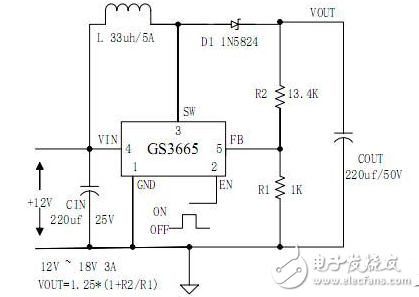
The GS3665 application circuit is very simple and has few peripheral components. And with enablepin for switching function, its internal complete system protection functions include adjustable soft-start, short circuit protection (SCP), over temperature protection (OTP) and adjustable overcurrent protection (adjustableOCP) function. The switching frequency is fixed at 400KHz.
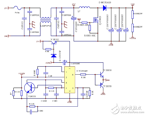
The figure below is a 24V to 110VBOOST boost circuit.
Three Phase Portable EV Charger
Three Phase Portable Ev Charger,Ev Home Charger,Portable Electric Charger,Electric Charger
Yangzhou JERI New Energy Co., Ltd. , https://www.jrevcharging.com