The 1.5V liter 9V power supply circuit diagram is shown in the drawing. This circuit is a batch oscillation boost circuit. BG1 and L1, L2, C1, etc. constitute an oscillator. BG1 is an oscillating tube and operates in a switching state. L1 and C1 are oscillation feedback elements. L2 is an oscillating energy storage winding. For convenience, the circuit also designed an automatic electronic switch composed of BG3. When the base of BG3 has no load, there is no base current, BG3, BG2, BG1 are all cut off, the whole circuit stops working, and no power is consumed. Therefore, this circuit does not require a separate power switch.
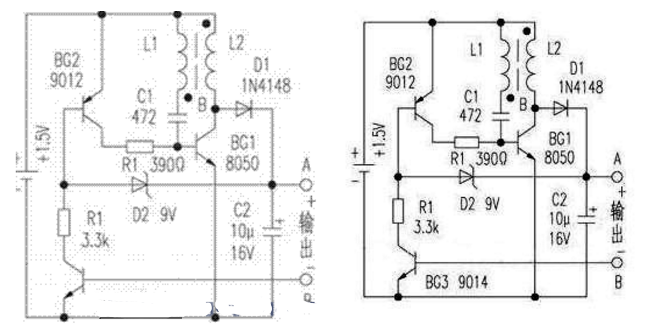
When the two points of A and B are connected to the load, BG3 is turned on, and BG2 is also turned on. The load supplies the base current to BG1, and BG1 is turned on. The energy flows in from the power supply and is stored in L2. At this time, the collector voltage of BG1 is very low, D1 is cut off, and the load is supplied by the residual voltage of C2. When BG1 is turned off, the current in L2 cannot be abruptly changed, and it will produce a higher counter-electromotive force, which is rectified by D1 and output. When the output voltage is higher than the regulation value of D2, the b and e junctions of BG2 tend to be reversed, and the base current of BG1 will decrease, forcing the oscillation to weaken, and the output voltage will also drop to automatically output the voltage. Control is near the regulation value of D2.
Component selection and production debugging:BG1 selects NPN type silicon tubes with reduced saturation voltage, such as 9013, 8050, etc., and requires ICM"300mA, β"200. BG2 can use PNP silicon tubes such as 9012 and 9015, and BG3 uses NPN type tubes such as 9014. The smaller the penetration current is, the better. L1 and L2 are wound on a 高频8MM high-frequency magnetic ring (detached from an old electronic ballast or energy-saving lamp) with a MM0.1MM enameled wire. L1 is 6åŒL2 is 36åŒ.
I use this circuit to supply power to the DT890A digital multimeter. The measured working current is: buzzer and capacitor 20uF, 2uF block is below 45mA, other gears are below 25mA. When the battery voltage drops to 0.9V, in addition to the buzzer block that consumes a large current, the capacitors 20uF and 2uF block have a power shortage display, and the remaining gears have no power shortage display. The circuit is simple to manufacture, stable in performance, economical and practical. No need to debug, as long as the wiring is correct, it can work normally.
Digital Multimeters If a 1.5V battery is used to replace a 9V stacked battery with a boost, it is usually necessary to install a separate power switch. Inconvenience to production and use. The circuit described in this article controls the start or stop by detecting the presence or absence of the digital multimeter's operating current. Therefore, as long as the power line is connected to the output of the booster circuit, the digital multimeter power switch can be used.
The simplest 9v boost circuit diagram (2)C1 is the role of positive feedback. When Q2 turns on, the positive feedback of C1 causes Q2 to quickly enter the saturation region. Then C1 discharges and reverses charging. As the base potential of Q1 increases, the base current of Q2 also decreases, and the current on L1 rises continuously. When it reaches a large enough Q2 to exit saturation, Q2 collector potential Raise, the positive feedback of C1 is given to the base of Q1 to increase the potential, so that Q1, Q2 will immediately return to the cut-off area. Q1 is turned on again, and it is necessary to recharge the R1 and C1 to lower the base potential of Q1. It takes a long time, so the charging time of the circuit L1 is usually much longer than the discharge (including waiting for recharging). Time.
When D1 is connected, the output voltage is too high, which will affect the charging and discharging of C1, resulting in shorter on-time of Q1 and Q2 and longer waiting time after discharge.
As can be seen from the above analysis, the operating frequency of this circuit is related to both R1 and C1. It is also affected by L1, but it has little effect.
The driving ability of this circuit is related to the value of R1, L1 and the amplification factor of Q1 and Q2.
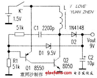
This circuit is easy to start, and the conditions for no vibration are:
R1 is relatively small. After Q1 and Q2 are turned on, C1 reverse charging is completed, and Q1 current reaches the minimum value. If Q2 is still in the saturation region (the internal resistance of L1 limits the collector current of Q2 to rise further), this It consumes a lot of power and the circuit stops.
A10 600 Puffs,A10 600 Puffs Box,A10 600 Puffs Disposable,A10 600 Puffs Disposable Vape
Lensen Electronics Co., Ltd , https://www.lensenvape.com