LF347 integrated circuit is cheap but reliable. This paper uses four operational amplifiers in LF347 to design a pulse width modulation control circuit, which has good control effect on DC output. It is divided into the basic structure of the circuit, the design analysis of each part of the circuit, and the output control.
First, the question is raised
Pulse width modulation control technology has been widely used in industrial control and home appliance circuits. In particular, due to the maturity of the PMW technology, the DC/AC inverter cost is greatly reduced, and the frequency conversion technology makes it easy to control the AC motor speed. However, is it possible to control the DC motor speed with pulse width modulation? Can the cost be reduced? I used a LF347 (4 op amp) to form a pulse width modulation controller to control the speed of the DC motor. Good results and low cost.
Second, the basic structure of the circuit
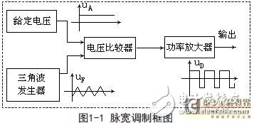
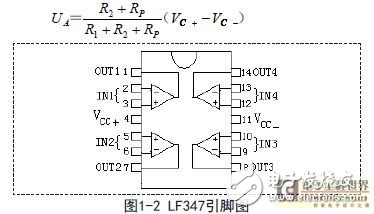
The circuit consists of four parts: a given voltage, a triangular wave generator, a voltage comparator, and a power output. The block diagram is shown in Figure 1-1, where an op amp is used for a given voltage section, two op amps are used for a triangular wave generator, and an op amp is used for a voltage comparator. Figure 1-2 shows the structure of the LF347 integrated circuit.
Third, the analysis of various parts of the circuit
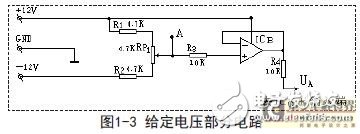
1. Given voltage portion
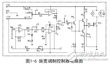
As shown in Figure 1-2, the given voltage part circuit consists of R1, RP 1, R2, and ICB. Adjust RP 1, adjust the potential of point A (+4V~-4V), and connect the ICB non-inverting input terminal through R3. Its inverting input is directly connected to the output, which is a voltage follower (voltage amplification is approximately equal to 1). This voltage is fed to the non-inverting input of the voltage comparator ICC:
2. Triangle wave generator
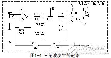
As shown in Figure 1-3, the triangular wave generator circuit consists of two operational amplifiers, ICD and ICA.
The ICD and the voltage regulators VD1 and VD2 form a rectangular wave generator, and the input terminal is in the form of a voltage comparator. When the "+" endpoint is higher than the "-" terminal, the output is a positive power supply voltage (about 12V); When the "+" endpoint is above the "-", the output is a positive supply voltage (approximately -12V). R15 is regulated by VD1 and VD2 voltage regulator (regulation voltage is 5V), and E-point can obtain rectangular wave (±5.7V) as the input signal of ICA.
ICA and C1, RP2, and R16 form an integration circuit. When the ICD output is a positive voltage, it is connected to the inverting input terminal of the ICA. The output is an integrated waveform from high to low. The voltage is divided by R15, R13, R14, and RP3. When the potential gradually drops and falls below the zero potential ("-" terminal is grounded), the ICD output is inverted to a negative voltage output, and the ICA output is an integrated waveform from high to low:
![]()
Thereby, the rectangular wave is changed into a triangular wave, and the F point is a triangular wave. The triangular wave is fed to the inverting input of the voltage comparator ICC.
Since the integral constant is 1/(RP+R16), the potentiometer RP2 can adjust the frequency of the triangular wave, and the RP2 has a small frequency; the potentiometer RP3 can adjust the amplitude of the triangular wave.
3. Voltage comparator
The operational amplifier ICC has no feedback components, so its amplification is extremely high and the output voltage jumps around ±10V.
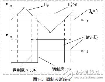
The inverting input sends a triangular wave UF, which is an alternating voltage that periodically changes with time. The non-inverting input is fed with a DC voltage UA, which does not change with time, and can be adjusted according to the load demand.
When UF UA, output -10V; when UF
It can be seen that when UA=0, the triangular wave UF outputs -10V in the positive half cycle; the triangular wave UF outputs +10V in the negative half cycle, and the modulation degree is 50%. The larger the UA, the longer the output is +10V. The degree of modulation increases; the smaller the UA is, the shorter the output is +10 V, and the degree of modulation decreases. Therefore, adjusting the magnitude of the given voltage UA is to adjust the output positive pulse width (modulation degree), and the average value of the output voltage can be adjusted. As shown in Figure 1-4.
4. Power amplifier
VT1, VT2, and VT3 form an OCL power amplifier. The output signal D point waveform is consistent with the input signal C point waveform, and is also a rectangular wave with adjustable pulse width.
VT4 is a field effect power tube, which is a voltage control element. When the gate G is applied with a negative voltage, ID=0, and it is turned off. When UG is greater than the cutoff voltage, the ID changes with UG, UG increases, and ID increases.
UG is the OCL output voltage UD, which is a rectangular pulse with ±10V transition. When positive pulse, VT4 is turned on. When negative pulse is used, VT4 is turned off, so the load current ID is positive pulse current.
By adjusting the given voltage UA, the positive pulse width of UC and UD can be changed, and the time when the load current ID appears is changed, and the average current and the average voltage of the load are changed to achieve the adjustment load-motor speed.
Fourth, debugging and conclusion
Through the debugging of the circuit, the triangular wave frequency is 1KHZ (adjusted RP2), and the amplitude is ±3V (adjusted to RP3). It is suitable to adjust the RP1 and A point potential (+4V~-4V) to make the pulse width modulation degree reach 0. %~100%. I installed it on the car and used it as the stepless governor of the air conditioner fan. It is convenient and suitable, but I need to add a LM7912 as the negative power supply.
Membrane switch is an operating system that integrates key functions, indicating elements and instrument panels. It consists of four parts: panel, upper circuit, isolation layer and lower circuit.
When the membrane switch is pressed, the contacts of the upper circuit are deformed downward, and are in contact with the pole plate of the lower circuit.
After the finger is released, the contacts of the upper circuit bounce back, the circuit is disconnected, and the circuit triggers a signal. The membrane switch has strict structure, beautiful appearance and good sealing performance. It has the characteristics of moisture resistance and long service life.
Widely used in electronic communication, electronic measuring instruments, industrial control, medical equipment, automobile industry, smart toys, household appliances and other fields.
Membrane Switch, Poly Membrane Switch, Home Appliance Membrane Switch, Membrane Switch with Leds, Membrane Switch Model
KEDA MEMBRANE TECHNOLOGY CO., LTD , https://www.kedamembrane.com