According to Moore's Law, in the next 10 years, continuing to increase the storage density and computing power of computers will face severe challenges. These challenges have both principled physical limitations and technical process limitations. Its main performance is as follows: â‘ When the size of electronic devices is in the order of micrometers, the electrons in them are mainly particle-like. But when the size of the device is as small as nanometers, the electrons are mainly fluctuating. The fluctuation of electrons is a quantum effect. At this time, electronic devices will work under a new principle; â‘¡ Any multi-body system has statistical fluctuations in heat. When the device size is reduced to nanometers, this thermal fluctuation Will limit the consistency of device performance, so that integrated chips can not work properly.
However, the emergence of nanoelectronic technology, nanoelectronic devices and nanoelectronics provides a new way and opportunity for the development of microelectronic technology. This aspect can be attributed to the continuous development of microelectronics and nanotechnology; on the other hand, it can be attributed to the potency of microelectronics and quantum physics on the preparation, characteristics, mechanism and characterization of nanoelectronic devices for more than half a century. stand by.
This article will analyze and elaborate the concepts of nanoelectronic devices and nanoelectronic technology, the classification of nanoelectronic devices and the existing nanoelectronic device preparation technologies. Finally, it points out several key problems that need to be solved urgently in nanoelectronics technology.
2 Nanoelectronic devices 2.1 Nanoelectronic devices and nanoelectronic technologies Nanoelectronic devices refer to nanoscale devices designed and prepared using nanoscale processing and preparation technologies, such as photolithography, epitaxy, microfabrication, self-assembly growth and molecular synthesis technology. (1% 100nm) scale and specific functions of electronic devices. At present, people have developed many nanoelectronic devices using nanoelectronic materials and nanolithography technology, such as electronic resonance tunneling devices (resonant diode RTD, tripolar resonance tunneling transistor RTT), single electron transistor (SET), metal-based SET, semiconductor SET, nanoparticle SET, single-electron electrometer, single-electron memory (SEM), single-electron logic circuit, metal-based single-electron transistor (SET) memory, semiconductor SET memory, memory made of silicon nanocrystals, nanofloating gate Memory, nano-silicon microcrystalline thin film devices and polymer electronic devices, etc.
Nanoelectronics technology refers to the construction of nanometer and quantum devices in the nanometer size range, integrating nanocircuits, thereby realizing the information calculation, transmission and processing of quantum computers and quantum communication systems. Among them, nanoelectronic devices are the current development of nanoelectronic technology. The key and core. Now, nanoelectronics technology is in a period of vigorous development, and its ultimate goal is to base on the latest physical theory and the most advanced technological means, break through the traditional physical size and technical limits, develop material potential information and structural potential, according to new concepts Design and manufacture nano-devices and construct electronic systems to achieve a revolutionary leap in the ability of electronic systems to store and process information.
2.2 Classification of nanoelectronic devices There are different views at home and abroad on the classification of nanoelectronic devices. According to the development of nanoelectronic technology and the prediction of the future, a division method broadly divides nanoelectronic devices into the following 8 categories: ①Nano-level CMOS devices, such as silicon MOS FET on insulating layer, heterojunction MOSFET, low temperature MOSFET Bipolar MOSFET, etc .; ② quantum effect devices, such as quantum interference devices, quantum dot devices, and resonant tunnel devices; ③ single-electron devices, such as single-electron boxes, capacitively coupled and resistance-coupled single-electron transistors, single-electron junction arrays, single-electron Pumps, single electron traps, etc .; ④Single molecule devices, such as single electron switches, single atom point contact devices, single molecule switches, molecular wires, quantum effect molecular electronic devices, electrochemical molecular electronic devices, etc .; ⑤ nanosensors, such as quantum tunneling Sensors, etc .; ⑥ Nano integrated circuits, including nano electronic integrated circuits and nano optoelectronic integrated circuits; ⑦ Nano memory, such as ultra-high-capacity nano memory, tunnel type static random access memory, single electron silicon-based MOS memory, single electron memory, single electron quantum Memory, etc .; ⑧ Nano CMOS hybrid circuit, including nano CMOS circuit and HV group compound semiconductor Resonant tunneling effect circuit, nano CMOS circuit and single electron nano switch circuit, nano CMOS circuit and carbon nano tube circuit, nano CMOS circuit and artificial atomic circuit, nano CMOS circuit and DNA circuit, etc. In this classification, nano-scale CMOS devices, nano-sensors, nano-memory, nano-integrated circuits, and nano-CMOS hybrid circuits are treated as an independent nano-device type.
But in fact, whether these nano-sensors, nano-scale CMOS devices or circuits should be included in the category of nano-devices is still controversial.
According to the two basic conditions proposed by David et al. In the category of nanoelectronic devices, that is, the working principle of the device is based on quantum effects; it has a typical structure of "islands" (or potential wells) surrounded by tunneling barriers. It is believed that although the scale of nano-sensors and nano-scale CMOS devices is in the order of nanometers, they have also been successfully developed using nano-processing technology, but they can only belong to the category of nano-devices and not the scope of nano-electronic devices. Based on this view, single electronic devices (SED); molecular electronic devices, mainly including quantum effect molecular electronic devices and electromechanical molecular electronic devices.
Should, that is, the wave-particle duality of electrons, nanoelectronic devices with various quantum functions are divided into two categories, namely â‘ single-electron devices, the electrons of these devices are in a point structure, and their behavior is focused on particle nature, typical Examples are single-electron transistors, single-electron switches, etc .; â‘¡ quantum wave devices. The electrons in such devices are in a phase-coherent structure, and their behavior is mainly fluctuating, mainly including quantum wire transistors, quantum interference devices, resonant tunnel diodes , Transistors, etc. In addition, considering the obvious differences in principle and material structure, molecular electronic devices are also juxtaposed with the above single-electron devices and quantum wave devices as a special class of nanoelectronic devices. The research of this kind of device belongs to the category of molecular electronics, including molecular electronic switches, electrochemical molecular devices. The preparation technology of 3 nanometer electronic devices has two possible ways to prepare nanoelectronic devices and implement their integrated circuits. One is to further extend the existing electronic devices and integrated circuits to miniaturization, and research and develop processing techniques with smaller line widths to process smaller-sized electronic devices, a so-called "top-to-bottom" method. Another way is to use advanced nanotechnology and quantum effects of nanostructures to directly constitute a brand new quantum device and quantum structure system, the so-called "bottom-up" approach.
The preparation method of nanoelectronic devices "from top to bottom" mainly refers to technologies such as optical lithography, electron beam lithography and ion beam lithography. "Bottom to top" preparation methods include metal organic chemical vapor deposition (MOCVD), molecular beam epitaxy (MBE), atomic layer epitaxy (AEE), chemical beam epitaxy (BE) and other epitaxy techniques, scanning probe microscope ( SPM) technology, molecular self-assembly synthesis technology and special ultra-fine processing technology, etc.
3.1 Lithography technology Optical lithography, electron beam lithography and ion beam lithography are collectively referred to as three-beam lithography, which is a 1C processing technology that transfers the designed device pattern structure to a semiconductor substrate through processes such as masks and exposure. At present, with the continuous reduction of the line width of lithography technology, optical lithography, electron beam lithography and ion beam lithography have shown good performance in the processing field of nano CMOS devices, nano integrated circuits, nano CMOS hybrid circuits, etc. Application prospects, and began to obtain applications in the processing of some nanoelectronic devices.
3.1.1 Optical lithography technology Optical lithography is a technology that uses a projection method to "engrave" the structure pattern of a large-scale integrated circuit device on a mask on a silicon wafer coated with photoresist through a projection method. It is now the mainstream technology for semiconductor processing in the 1C industry. In this technique, methacrylate polymer (PMMA) is usually used as a resist coating, and a mixture of methyl isobutyl ketone and isopropyl alcohol is used as a developer.
At present, the most interesting hot spot in the international microelectronics field is the new generation of lithography technology. With the processing size to 0.1! m is approaching, can it break through 0.1! m has become the most severe challenge facing the existing optical lithography technology. The minimum line width that can be obtained by limiting lithography is directly related to the resolution of the lithography system, and reducing the wavelength of the light source is the most effective way to improve the lithography resolution. Now, the wavelength of the light source of the commercial lithography machine has entered the deep ultraviolet band from the ultraviolet band of the mercury lamp light source in the past, and it can be obtained by using ArF excimer laser with a wavelength of 193nm as the light source. 0.18! The lithographic line width of m.
In addition, extreme ultraviolet lithography (EUVL, also known as soft X-ray lithography) and X-ray lithography techniques that use shorter wavelength extreme ultraviolet light (wavelength 109 14nm) and XRL light (1nm) as light sources have also been developed . According to the current development situation of lithography technology, EUVL will likely become the mainstream technology for mass production of integrated circuits with feature sizes of 70nm and finer line width. According to the blueprint for the development of semiconductor technology released by the International Semiconductor Industry Association in 2001, semiconductor electronic devices with a characteristic line width of 70 nm are likely to enter mass production in 2006.
In addition, the in-depth analysis of exposure imaging using the interference characteristics of light and electromagnetic theory combined with the actual lithography, and the use of various wavefront techniques to optimize process parameters are also important means to improve lithography resolution.
Electron beam lithography (EBL) Electron beam lithography is a lithography technique that uses high-energy electron beams to expose a photoresist to obtain a structure pattern. Since the De Broglie wavelength of the electron beam is about 0.004 nm, which is much smaller than the wavelength of the lithography technique, therefore, the electron beam lithography is hardly affected by the diffraction limit, and resolution close to the atomic scale can be obtained. Now, EBL has not only become an indispensable mask making tool in VLSI manufacturing, but also a main method for processing nano devices and nano structures.
At present, the resolution of the electron beam exposure machine has reached 0.1! m or less. However, the production efficiency of electron beam lithography is very low, only 5 to 10 wafers per hour, which is much lower than the current 50 to 100 wafers per hour of optical lithography, so it has become a "bottleneck" restricting its wide application ".
Recently, the SCALPEL technology of angle-limiting scattered projection electron beam lithography developed by Lucent Corporation of the United States has attracted attention. This technology reduces the projection of the mask pattern like optical lithography, and uses special filtering technology to remove scattered electrons generated by the mask absorber , So as to improve output efficiency while ensuring resolution. It should be pointed out that no matter what technology is used in future lithography, EBL will be an indispensable infrastructure for integrated circuit research and production.
Ion beam lithography (IBL) ion beam lithography is a lithography technique that uses liquid atoms or gas atoms to ionize nano-devices and ions formed by mm after exposing the photoresist after electromagnetic field acceleration and electromagnetic lens focusing or collimation. The principle is similar to electron beam lithography, but De Broglie has a shorter wavelength, and has the advantages of no proximity effect and large exposure field. Ion beam lithography mainly includes focused ion beam lithography (FIBL), ion projection lithography (IPL), etc. Among them, FIBL developed earliest, and has recently obtained a resolution of 10 nm in experimental research. However, the efficiency of this technology is extremely low, and it is difficult to be used as an exposure tool in production. At present, it is only used for mask repair tools and special device repairs in VLSI.
Due to the shortcomings of FIBL, people are now starting to develop IPL technology with higher exposure efficiency. For example, a large number of enterprises, universities and research institutes in Europe and the United States have launched a cooperative project called MEDEA to solve bottlenecks in equipment and masks.
3.2 Epitaxy Metal organic chemical vapor deposition (M0CVD), molecular beam epitaxy (MBE), atomic layer epitaxy (AEE) and chemical beam epitaxy (BE) are collectively referred to as epitaxy technology, which is a kind of nanometer that grows nanometer film on the substrate The manufacturing technology can be used for the processing and preparation of silicon-based semiconductor materials (SoI) for nano integrated circuits and nano semiconductor structures / devices.
The principle diagram of molecular beam epitaxy technology is given.
Place the substrate (usually Si-based substrate) and multiple molecular beam jet furnaces relatively in an ultra-high vacuum system to combine various elements (such as' (8, etc.) and The dopant elements (eg, B, etc.) are placed in different spray furnaces and heated so that their molecules are sprayed onto the surface of the heated substrate at a certain thermal motion speed and a certain beam intensity ratio, and finally interact with the surface The epitaxial growth of single crystal thin film is performed. The baffle in front of each spray furnace is used to change the composition and doping of the epitaxial film. According to the set program, the baffle is switched, the furnace temperature is changed and the growth time is controlled, then different thicknesses can be grown Compounds or ternary and quaternary solid solutions with different composition ratios and their heterojunctions, thereby preparing various ultra-thin microstructure materials.
At present, the most common silicon-based semiconductor materials for nano-integrated circuits using epitaxial growth are silicon-on-insulator (SoI) materials and silicon-germanium (Si'e) heterogeneous materials. SoI and Si 'heterogeneous materials and derived new silicon-based semiconductor materials have begun to be applied to various micro-nano electronic devices and integrated circuits because they can meet the circuit requirements of low voltage, low power, high speed, and radiation resistance.
MBE, MOCVD, ALE and other epitaxial technologies can meet the design accuracy requirements, such as epitaxial layer composition, thickness, doping concentration, and electrical uniformity, so that various high-quality superlattice quantum well materials can be grown.
In addition, by using selective epitaxy on the surface of the V-groove or step surface, horizontal epitaxy with stripe mask selection, strain-induced restricted epitaxy, and laser-assisted atomic beam epitaxy, various low-level epitaxy techniques with special functions One-dimensional nanostructures, such as one-dimensional quantum wires and zero-dimensional quantum dots.
3.3 Molecular self-assembly synthesis technology Self-assembly is a process that relies on intermolecular non-covalent bonding forces to spontaneously combine into stable aggregates. Since the concept of molecular devices was put forward in the 1980s, people have developed from LB technology to molecular self-assembly technology, from dual liquid membrane (BLM) technology to SBLM technology, and have assembled ordered molecular films and processed molecules with specific functions in molecules. The aggregate has achieved fruitful results. For example, the Department of Chemistry of Massachusetts University of Technology uses self-assembly technology of colloidal crystals to synthesize CdS nanocrystal three-dimensional quantum dots; Aliviatos et al. Use metal colloidal nanostructure self-assembly technology to self-assemble Au nanoparticles through Aaton-Crick base pairing Onto the DNA molecule, forming a "nanocrystalline molecule"
; Yang et al. Used porous nanostructure self-assembly technology to mix TEOS with acidic aqueous solution of chlorohexadecyl trimethyl plating, and then allowed it to grow nucleated at 80K on the surface of fresh cleaved mica , Obtained mesoporous SiL film with continuous orientation growth.
In recent years, molecular self-assembly technology has also been used by many scientists to synthesize nanostructured materials with specific electronic properties. These nanostructures synthesized by molecular self-assembly mainly include nanorods, nanotubes, multilayer films and mesoporous materials. For example, Li et al. Successfully synthesized nanotubes with a length of 20-35nm and a diameter of 2nm through the connection of diphenylhexatriene with cyclodextrin; workers at the University of Illinois in the United States successfully synthesized mushroom-shaped polymers Aggregates, and using this as a structural unit, self-assembled supramolecular multilayer membranes with nanostructures; Fuita et al. Prepared hollow molecules that did not exist in nature by self-assembly using 4 organic ligands and 6 metal Pd ions Mesoporous supramolecular, etc.
Since the birth of the first scanning tunneling microscope (STM) in 1982 and the subsequent invention of various scanning probe microscopes, humankind has opened a new page in the world of micro / nano view. SPM can not only perform high-resolution three-dimensional imaging and measurement, but also study the different properties of materials. Therefore, it is not only a microscopic measurement and analysis tool, but also an important microscopic processing and manipulation tool.
SPM probes are used to directly scribe nano-patterns on the sample surface or toggle particles to a designated place to construct specific nanoelectronic devices / structures. This technology generally requires the use of special SPM probes. The tip of the probe is generally hard diamond particles. The probe cantilever requires a material with a high elastic modulus, usually up to 20N / m. Such as the self-developed by Chen Haifeng of Peking University. The AFM etching system successfully scribed nano-scale holes, grooves and various complex patterns on the Au-Pd alloy film.
The combination of scanning probe technology and other technologies can manipulate control molecules and atoms, process micro-scale mechanisms at the nanometer scale, and can even be used to design, manufacture, and assemble new quantum devices and equipment. In recent years, scientists have achieved many important results in this area, and have designed single-electron switches, single-electron transistors, single-electron logic devices, carbon nanotube rectifiers, molecular switches, chemical molecular motors, and nano-locks and nano-keys processed with AFM Wait.
3.5 Special ultra-fine processing technology There are also some special ultra-fine processing technologies that can be used to process and prepare nanoelectronic devices. They include mechanically controlled crack connection electrode technology to prepare Au atomic wires; carbon nanotubes to construct FETs; using DNA molecules, carbon nanotubes, and mesoporous materials as templates to prepare quantum wires, ultra-precision composite processing, electrolytic jet processing, and electrical discharge machining Electrochemical processing technology, etc.
4 Some key issues that need to be solved urgently in nanoelectronics technology. Because the feature size of nanodevices is in the order of nanometers, the mechanism is very different from existing electronic components. There are many quantum phenomena and related problems in theory that need to be solved. Tunneling process in the well, mechanism of inelastic scattering effect, etc. Nonetheless, the key issues that need to be solved urgently in nanoelectronics mainly lie in the nanoelectronic technology related to nanoelectronic devices and nanoelectronic circuits, which are mainly manifested in the following aspects.
To continue to shrink the existing silicon-based electronic devices to the nanometer scale, the most straightforward method is to use epitaxy, photolithography and other technologies to manufacture a new generation of layered cake-like nano-semiconductor structures.
Among them, the different layers are usually made of semiconductor materials with different potential energy, which are built into nano-scale quantum potential wells. This structure is called "semiconductor heterojunction". However, it is usually difficult to manufacture stable and reliable semiconductor heterojunctions at the nanometer scale from the current state of the art. Therefore, it is necessary to develop high-performance nano-Si-based quantum heterojunction processing technology as soon as possible.
Molecular transistors and wire assembly Even if you know how to make molecular transistors and molecular wires, assembling these components into a working logical structure is still a very difficult problem. One possible way is to use a scanning tunneling microscope to arrange the molecular elements on a plane; another possible way to assemble larger electronic devices is through array self-assembly. Although research institutions such as PurdueUniversity have made gratifying progress in this direction, it is still impossible to say when the technology will get out of the laboratory and become practical.
Ultra-high-density quantum effect memory micro-nano electronic technology Ultra-high-density storage quantum effect electronic "chip" is the main component of future nanocomputers, it can provide mass storage for computer information systems with fast access capabilities but no moving mechanical parts means. However, with the ability to manufacture nanoelectronic logic devices, how to use such devices to assemble ultra-high-density storage quantum effect memory arrays or chips also poses new challenges for nanoelectronics researchers.
Nanocomputer's "interconnection problem"
A nanocomputer assembled from trillions of nanoelectronic components in an unprecedented density is destined to require a clever structure and a reasonable overall layout. Among the overall structural problems, the so-called "interconnection problem" needs to be solved first. In other words, it is the input / output problem of information in the calculation structure. To store massive amounts of information in a small space and use and generate information extremely quickly, a nanocomputer needs a special structure to control and coordinate many components of the computer. Between nanocomputing components, computing components, and the external environment There needs to be a lot of connections. As far as the miniaturization of existing traditional computer designs is concerned, since the wires must be separated from each other to avoid overheating or "stringing", there are some geometric considerations and restrictions, and the number of connections cannot be increased without limit. Therefore, the quantum tunneling effect between nanocomputer wires and the "connection" between wires and nanoelectronic devices urgently need to be resolved.
SPM nanodevice processing technology efficiency SPM technology provides a new way for the processing and preparation of nanoelectronic devices. Nanoelectronic devices will eventually become practical and economically feasible, requiring nanostructures to be assembled quickly and in large quantities. However, the current processing technology using SPM nanodevices is extremely inefficient, so it is not enough to assemble one nanostructure at a time with only one micro-scanning tunnel microscope or micro-atomic force microscope. If nanoelectronic devices are to be assembled mechanically, a large number of highly efficient parallel microscopic "nanomanipulators" are required to complete.
Nano / molecular electronic device preparation, manipulation, design, performance analysis and simulation environment At present, molecular mechanics, quantum mechanics, multi-scale computing, computer parallel technology, and computer graphics have achieved rapid development. Use these technologies to build a nanoelectronic device preparation , Simulation, virtual environment of manipulation, design and performance analysis, and it has become possible for nanotechnology researchers to get a virtual experience. However, due to the problems of the speed of existing computers, the efficiency of molecular mechanics and quantum mechanical algorithms, there are still great difficulties in establishing such a fast, sensitive and precise quantum simulation virtual environment.
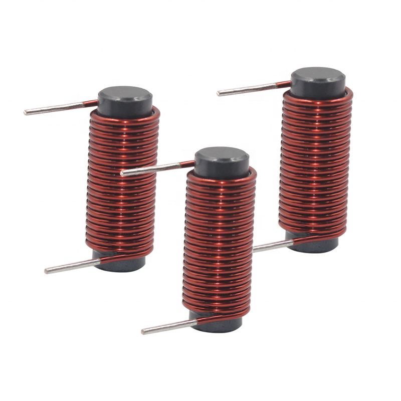
Rod core coil is winding the copper wire onto a Mn-zn or Ni-Zn Ferrite Core. Their features are high current capacity, low core loss at frequency and high magnetic saturation. Customized designs available for different request Applications. They usually be used in Switching regulators, Motors, Power amplifiers, Power supplies, Broadband filtering, Typical in VHF.

| Mode: | Air inductor ferrite rod antenna used for radio antenna, LF/HF RFID antenna/Rod core induction coil |
| Material: | NiZn,MnZn, soft ferrite rod core. |
| Application |
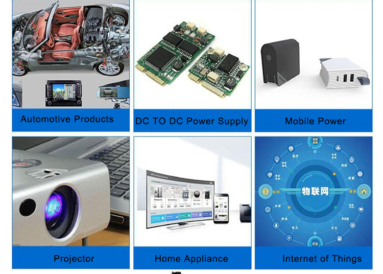
Led light driver, GPS,Computer,Audio/video components, Electric PCB board,switch,various current circuits,filters,AC adapter,air conditioning,Car Ignitor,...ETC |
| Inductance: | 1uH-1H |
| IDC: | 0.1A-30A |
| Certificated: |
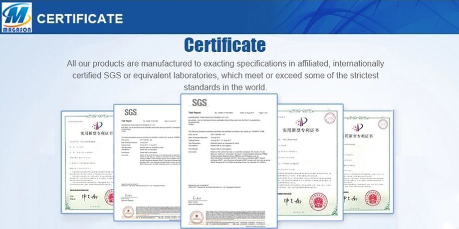
ISO9001-2015, SGS-ROHS. |
| MOQ: | No MOQ for the trial order. |
| Samples/Delivery: | 1-5pcs free samples for freight collect. /5-10days. |
| Type of payment: | T/T, Western Union, L/C, Alipay,Paypal,etc. D/A/... |
| Features: | Inductors,high current RF transformer made with soft ferrite core, include NiZn, MnZn, Amorphous, Iron powder metal core for winding, tinned, guled,content toroidal inductor, rod inductor, drum inductor,smd chip inductor coil,widely used in many PCB boards, for filers, EMI/EMC, Anti-noise,Amplifier,RF transformer,..... |
| Advantage: |
1.Ferrite core and inductor Factory. 2.Good quality products with factory price. 3.Enough production capacity provide good delivery time. 4.Special products customized accepted. 5.Good aftersales services. |


Rod Core Coil,R Bar Coil,Rod Core Choke,Magnetic Rod Inductor
Shaanxi Magason-tech Electronics Co.,Ltd , https://www.magason-tech.com