51 single-chip interrupt system is very important, divided into external interrupts and timer interrupts. This article mainly explains the interrupt system architecture and the interrupt response process of the 51 single-chip microcomputer, specifically follow the small series together to find out.
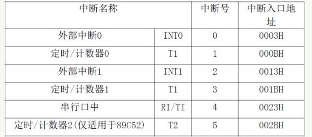
51 single-chip interrupt system architectureThe 80C51 interrupt system has 5 interrupt sources (6 of 8052) and 2 priority levels, enabling nested interrupts. The mechanism of the MCS-51 series microcontroller interrupt system is as follows:
Special registers related to the interrupt system:
1) Interrupt Enable Control Register (IE) ------ Controls the opening and masking of each interrupt
2) Interrupt priority control register (IP) ------ set the priority of each interrupt
3) Timer/Counter Control Register (TCON) ---- Timer and External Interrupt Control
4) Serial Port Control Register (SCON) ------ Serial Interrupt Control
The types of interruptions fall into three categories:
1) T0, T1 are two timer / counter interrupts, provided by the on-chip timer;
2) INT0, INT1 are two external interrupts, provided by pins P3.2 and P3.2;
3) RX, TX are used for serial port interrupts and are provided by on-chip serial ports.
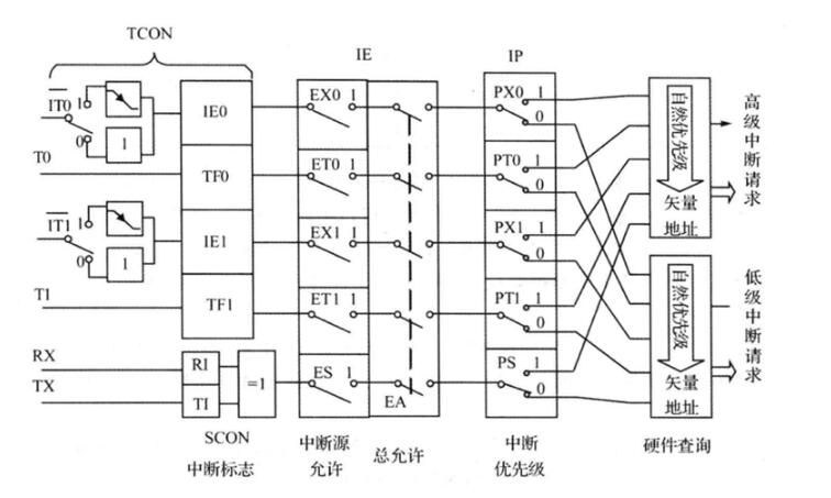
1. (P3.2)/(P3.3) It can be selected by IT0(TCON.0)/IT1(TCON.2) to be active low or active. When the CPU detects a valid interrupt signal on the P3.2/P3.3 pin, the interrupt flag IE0 (TCON.1)/IE1 (TCON.3) is set and the CPU requests an interrupt.
2. TF0 (TCON.5)/TF1 (TCON.7), on-chip timer/counter T0/T1 overflow interrupt request flag. When the timer/event counter T0/T1 overflows, TF0/TF1 is set and an interrupt is applied to the CPU.
3, RI (SCON.0) or TI (SCON.1), serial port interrupt request flag. When the serial port receives a frame of serial data, it asserts RI or when the serial port sends a frame of serial data, sets TI to request an interrupt from the CPU.
1) Use of Timer Interrupt (Take timer 0 as an example)
......
TMOD |= 0x01 | 0x04; //Using mode 1, 16-bit counters, using the "|" sign can be unaffected when using multiple timers
TH0=0xFF; // given initial value
TL0=245; //count from 245 to 255
EA=1; // total interrupt is on
ET0=1; // Timer interrupt open
TR0=1; //The timer switch turns on
Void Timer0_isr(void) interrupt 1 using 1 //Interrupt Service Routine
{
TH0=0xFF; //Reset initial value
TL0=245;
......
}
2) Use of External Interrupts (External Interrupt 0 as an example)
............
EA=1; // Globally disconnected
EX0=1; //External interrupt 0 open
IT0=0; //Level trigger
Void ISR_Key(void) interrupt 0 using 1 //Interrupt service routine
{
............
}
Interrupted response processIf an interrupt source is set by programming, it is in the opened state and the conditions for the interrupt response are met, and 1 the instruction currently being executed has been executed.
1, the current end of the response peer or senior interrupt
2. The MCU responds to this interrupt if it is not operating IE, IP interrupt control register or executing REH instruction.
In a normal situation, from the start of the interrupt request signal to the effective reception of the interrupt, it usually takes 3 machine cycles to 8 machine cycles. After the interrupt is acknowledged, the interrupt request flag (interrupt flag to the serial I/O port, cleared by software) is automatically cleared and the breakpoint, the program counter value (PC), is pushed onto the stack (for recovery purposes); Load the PC with the corresponding interrupt entry address and transfer the program to the corresponding interrupt service routine for execution.
The interrupt entry address of each interrupt source in program memory is as follows:
Interrupt source entry address
INT0 (external interrupt 0) 0003H
TF0 (TO interrupt) 000BH
INT1 (external interrupt 1) 0013H
TFl (T1 interrupt) 001BH
RI/TI (serial port interrupt) 0023H
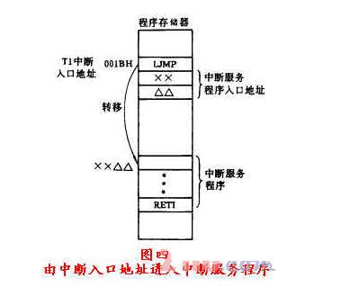
Because each interrupt entry address is very close to each other, it is not convenient to store each longer interrupt service routine. Therefore, a transfer instruction is usually arranged in the two or three units of the interrupt entry address to transfer to the interrupt service arranged there. program. Take the T1 interrupt as an example. The process is shown in Figure 4.
Since the five interrupt sources each have their interrupt request flags 0, TF0, IEl, TF1, and RI/TI, each flag is automatically set to 1 to request an interrupt from the CPU when the interrupt source satisfies the interrupt request. If an interrupt source raises an interrupt request, the CPU cannot respond immediately. As long as the interrupt request flag is not cleared manually by the software, the interrupt request status will remain until the CPU responds to the interrupt. For the serial port interrupt, The difference between this process and the other 4 interrupts is that even if the CPU responds to the interrupt, its interrupt flag RI/TI will not be automatically cleared, and it must be set in the interrupt service routine to clear the RI/TI instruction. Once again, an interrupt request is made.
The on-site protection and recovery of the CPU must be completed by the corresponding interrupt service routine. When the RETI interrupt return instruction is executed, the breakpoint value is automatically popped off the top 2 bytes of the stack and loaded into the PC register so that the CPU continues to be executed. Broken program.
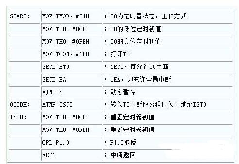
An example of applying a timer interrupt is given below.
It is required to compile a program to make the P1.0 port output a square wave pulse with a period of 2ms. SCM frequency
Fosc=6MHZ.
1. Method: Use timer T0 for 1ms timing to cause an interrupt after the timer value is reached. In the interrupt service routine, the state of P1.0 is taken once and the timing is again 1ms.
2, timing initial value: machine cycle MC = 1 / fosc = 2us. Therefore, the number of machine cycles required for timing lms is 500D, which is 0lF4H. Let T0 be the working mode 1 (16-bit mode), the initial timing value is (01F4H) complement = FEOCH
Serial Port Control Registers:
The serial port has a total of 2 control registers, SCON and PCON, used to set the serial port's operating mode, receive/send operation status, receive/send data characteristics, baud rate size, and the interrupt flag as the operation.
1 serial port control register SCON
The byte address of SCON is 98H, and the bit address (from low to high) is 98H to 9FH, respectively. The SCON format is shown in Figure 5.
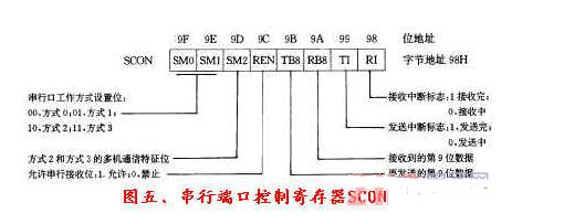
SMo, SMl:
Serial port operation mode control bit.
00--Method 0; 01--Method 1;
10--style 2; 11--style 3.
SM2:
Multi-machine communication control bits for mode 2 and mode 3 only
Transmitter SM2=1 (requires programming setting).
When Mode 2 or Mode 3:
When the receiver SM2=1, if RB8=1, serial receive interrupt can be caused; if RB8=0, no
Causes serial receive interrupt. When SM2=0, if RB8=1, serial receive interrupt can be caused;
RB8 = 0 can also cause serial receive interrupts.
REN:
Serial receive enable bit.
0--Disable reception; 1--Allow reception.
TB8:
In modes 2 and 3, TB8 is the 9th bit data to be sent by the transmitter.
RB8:
In modes 2 and 3, RB8 is the 9th bit data received by the receiver, which is exactly from the
Send the TB8.
TI:
Send interrupt flag. Must be cleared by software before sending, and TI keeps at zero level during sending.
After sending a frame of data, it is automatically set by hardware. If you want to send it again, you must clear it again with software.
RI:
Receive interrupt flag. Before receiving, it must be cleared by software. During the receiving process, RI maintains zero level. After receiving a frame of data, it is automatically set by the on-chip hardware. If you want to receive it again, you must use software to clear it again.
Power Control Register PCON
PCON byte address is 87H, no bit address, PCON format shown in Figure 6. It should be pointed out that PCON has several effective control bits for the 80C31 microcontroller.

SMOD: baud rate doubled. When calculating the baud rate of serial mode 1,2,3; 0 --- not doubled; 1 --- doubled.
H-K9L (N-BK7) is crystal clear and has excellent transmittance from visible to near infrared (350-2000nm). It is the most commonly used optical glass for the preparation of high-quality optical components. When the additional advantages of UV fused silica are not required (in When the ultraviolet band has good transmittance and low thermal expansion coefficient), H-K9L is generally selected for optical coating and other fields.
The ball lens is a very useful optical element used to improve the signal coupling between the fiber, the transmitter and the detector. In addition, it is also suitable for applications such as endoscopes, barcode scanning, pre-processed materials for Aspheric Lenses and sensors. The ball lens is made of a single glass substrate and can focus or output parallel light, depending on the geometry of the input source. Hemispherical lenses are also very common, and are used interchangeably with (full) spherical lenses when the physical constraints of the application require a more compact design.
H-K9L Ball Lens,N-Bk7 Ball Lens,H-K9L Optical Ball Lens,High Precision Ball Lens
Bohr Optics Co.,Ltd , https://www.bohr-optics.com