The rectification and filtering circuit, the AC-DC conversion circuit, and the DC-DC voltage conversion conversion circuit constitute the subject of this research. Rectifier filter circuit and AC-DC converter circuit: consisting of filter capacitor, isolation transformer, bridge rectifier stack and other components, to achieve 15 ~ 20V output voltage on the secondary side of the isolation transformer, after filtering to provide DC-DC 18-26V DC Input voltage. DC-DC conversion circuit: It is a pulse width modulation circuit composed of UC3843 and its peripheral circuits, Schottky diode, power inductor, fast power FET, etc. The system forms a closed loop feedback loop by adjusting the sampling resistor. The system has the advantages of high precision, low voltage adjustment rate, fast adjustment speed, high efficiency, small output ripple, etc., and achieves very good functions.
1 The design of the regulated Power Supply shows that the types of DC-DC conversion are divided into: isolated and non-isolated. Although the input and output isolation is relatively high, the isolation transformer has disadvantages such as magnetic flux leakage and loss, which will cause efficiency degradation. According to the requirements of this study, input and output isolation is not required, so the final decision is to choose non-isolated mode. Several options are as follows:
1.1 The series switching circuit has a duty cycle of D. The PWM wave controls the switching transistor Q1 to achieve such an effect, alternately turning on or off, and then obtaining a stable DC output voltage Uo on the load R via the L and C filters. This circuit is a step-down type circuit, and the output voltage of 30--36V required by the problem cannot be realized.
1.2 Parallel Switch Circuit The series switch circuit is similar to the parallel switch circuit principle, but this circuit is a boost type circuit. When the switch is turned on, the inductor starts to store energy. When the switch is turned off, the inductor energy starts to output. Therefore, as long as the inductor winding is reasonable, it can reach the demand of 30-36V, and the output voltage Uo exhibits continuous smoothing characteristics. (figure 1) 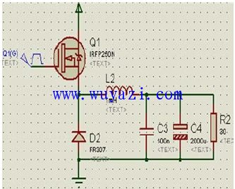
figure 1
1.3 Series-parallel switch circuit The following is a series-parallel switch circuit form, also known as buck-boost switch circuit, reverse switch circuit. This circuit can function regardless of the pulsating DC voltage before the switching transistor VT1, higher or lower than the stable voltage at the output. In fact, this circuit is in series with a switching circuit that is followed by a parallel switching circuit. The energy storage characteristics of the inductor are used to realize the buck-boost, and the circuit control type is relatively complicated.
Considering that this design only needs to be boosted, choose option two. (figure 2) 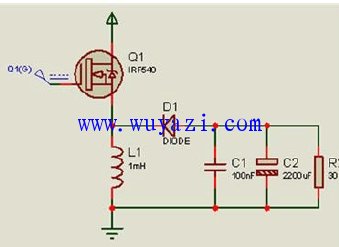
figure 2
2 unit circuit design and analysis 2.1 AC-DC conversion circuit (Figure 3) 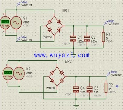
image 3
2.2 parallel switch circuit (Figure 4) 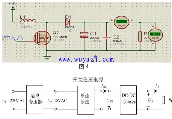
Figure 4
3 General schematic diagram and component list 3.1 General schematic diagram (Figure 5) 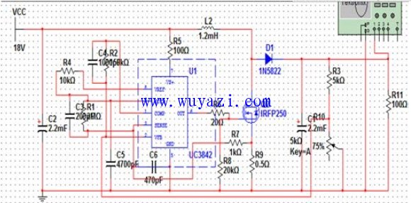
Figure 5
3.2 Working principle This design is to convert the 220V mains through buck rectification and filtering to obtain a relatively stable DC voltage. The DC voltage is boosted by Boost boost chopper circuit and filtered to obtain smooth DC output. At the same time, UC3843 output PWM The signal drives the switch tube to control closed loop feedback. In the research, the voltage divider circuit is adjusted to stabilize the output voltage between 30 and 36V. When the output voltage is increased, the feedback amplifier and the reference voltage are compared, and the output of the error amplifier is increased, thereby narrowing the output pulse width and shortening the switch. The tube conducts time, thereby reducing the output voltage. By the same token, when the output voltage is lowered, the error amplifier output is reduced after the reference voltage and the feedback signal are compared, so that the output pulse width is widened, the on-time of the switch is made longer, and the output voltage is increased. Therefore, the final result of closed-loop feedback regulation is to stabilize the output voltage between 30~36V. And, the circuit has an overcurrent protection function. When the output current is greater than 2A, the output of the error amplifier will also increase, and the output voltage will decrease, which will act as a current limiting function to protect the FET.
3.3 List of components (Figure 6) 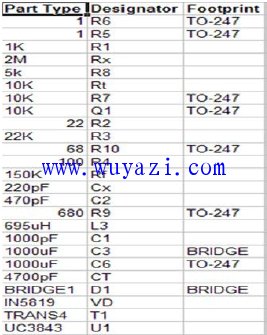
Figure 6
4 Conclusions and Results The system realizes the regulated output of the BOOST boost chopper circuit through the UC3843 pulse width controller. Through the rectification and filtering circuit, the overcurrent protection circuit, and the regulation of the DC-DC converter circuit voltage feedback circuit, the Boost is realized. The boost chopper circuit smoothly adjusts the input voltage of 220V. The mains output is adjustable between 30~36V.
Super Millionaire 3 Kit,super millionaire,juegos infantiles,slot machine kit
Guangzhou Ruihong Electronic Technology CO.,Ltd , https://www.callegame.com