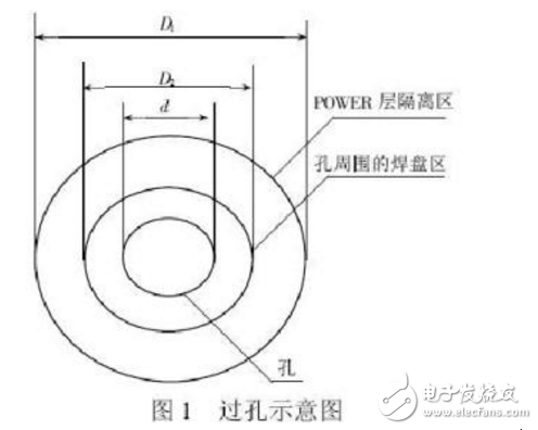
1, via
Via is called a via, and has a through hole, a blind hole and a buried hole. It is mainly used for the connection of wires of different layers in the same network, and is generally not used as a soldering component. among them:
1) Blind holes are used for the connection of the surface line and the inner layer line (only in the multi-layer board, only one head of the hole can be seen, and the other head does not penetrate the board).
2) The buried hole is the connection between the inner layer and the inner layer (only in the multilayer board, the buried hole cannot be seen outside)
3) The through hole is a hole penetrating the surface layer and the bottom layer for internal interconnection or as a mounting hole for the component.
The only connection for the connection of the line is the commonly used via hole, which is small in size. The holes used to mount the soldering elements are generally larger than the vias.
The vias consist of drill holes and pads.
The simplest understanding is that the pad is a larger hole for the soldering component. The pilot holes are small, only the holes that connect the different layers of the wires.
Both professional and simple:
1) A via is a hole that is connected between a double layer or a plurality of layers and a layer; it is characterized by electrical continuity and is not used for soldering;
2) Drilling is a mechanical hole on the PCB, used for assembly, not necessarily electrical properties, and can not be welded;
3) The pad is a perforated or gold-plated surface (surface pad SMD PAD) used to secure the electronic device. It is characterized by electrical continuity and can be soldered.
2, pad
The pad is called a pad, and has a pin pad and a surface pad. The pin pad has a solder hole, which is mainly used for soldering the pin component, and the surface pad has no solder hole, and is mainly used for soldering the surface mount component.
3, via mainly plays the role of electrical connection, the aperture of via is generally small, usually as long as the plate processing technology can be done, and the via surface can be coated with solder resist ink or not; To the role of electrical connection, but also mechanical fixation, the aperture of the pad (of course, the pin pad) must be large enough to pass through the component's pins, otherwise it will cause production problems; in addition, the pad surface must be There can be no solder mask ink, as this will affect the soldering, and it is common to apply flux on the pad surface when making the board; and the aperture between the aperture of the pad (when it refers to the pin pad) must also be between the aperture and the aperture. Meet certain standards, otherwise it will not only affect the welding, but also lead to the installation is not strong.
Second, the difference in processing methods1. How much is the hole in the VIA design, and how much is the hole. Then go through the process steps such as sinking copper, and the final actual aperture will be about 0.1mm smaller than the design aperture. For example, the via hole is set to 0.5 mm, and the actual aperture is only 0.4 mm. 2. The diameter of the PAD will increase by 0.15mm when drilling. After the copper sinking process, the aperture is slightly larger than the design aperture, about 0.05mm. For example, if the design aperture is 0.5mm, the hole diameter will be 0.65mm, and the finished hole diameter is 0.55mm.
3. VIA will cover green oil in some default PCB processes, which may be blocked by green oil and cannot be soldered. The test point can't be done either.
4, VIA welding ring minimum width of 0.15mm (in the case of general process), in order to ensure reliable copper plating.
5, PAD welding ring minimum width of 0.20mm (in the case of general process), in order to ensure the adhesion of the pad.
Pressure Type Liquid Level Sensor
It is suitable for liquid level measurement of various media in petrochemical, metallurgy, electric power, pharmaceutical, water supply and drainage, environmental protection and other systems and industries. The exquisite structure, simple adjustment and flexible installation provide convenience for users to use easily. Standard signal output modes such as 4 ~ 20mA, 0 ~ 5V and 0 ~ 10mA are optional by the user according to needs. Using the principle of hydrostatics to measure liquid level is an important application of pressure sensor. The special cable with ventilation duct in the middle and special sealing technology are adopted, which not only ensures the water tightness of the sensor, but also connects the reference pressure chamber with the ambient pressure, so as to ensure the high precision and high stability of the measurement.
Pressure Type Liquid Level Sensor,Liquid Water Level Sensor,Liquid Level Mearurement Sensor,New Pressure Type Liquid Level Sensor
Taizhou Jiabo Instrument Technology Co., Ltd. , https://www.jbcbyq.com