As integrated circuit output switching speed increases and PCB board density increases, signal integrity has become one of the issues that must be addressed in high-speed digital PCB design. The parameters and components of the components and PCBs are laid out on the PCB board. Factors such as the wiring of high-speed signal lines can cause signal integrity problems. For PCB layout, signal integrity needs to provide a circuit board layout that does not affect signal timing or voltage, and for circuit wiring, signal integrity. Termination components, layout strategies, and cabling information are required. High signal speeds on the PCB, improper layout of termination components, or improper routing of high-speed signals can cause signal integrity problems, which may cause the system to output incorrect data, the circuit is not working properly, or even does not work at all. Considering the factors of signal integrity and taking effective control measures during the design process has become a hot topic in today's PCB design industry.
1. Signal integrity issues
Good signal integrity means that the signal can respond with the correct timing and voltage level values ​​when needed. Conversely, signal integrity problems arise when signals do not respond properly. Signal integrity problems can lead to or directly result in signal distortion, timing errors, incorrect data, address and control lines, and system malfunctions, or even system crashes. Signal integrity issues are not caused by a single factor but in board-level design. Caused by a variety of factors. The IC's switching speed, incorrect layout of termination components, or miswiring of high-speed signals can cause signal integrity issues. The main signal integrity issues include: delay, reflection, synchronous switching noise, ringing, ground bounce, crosstalk, and so on.
2. Definition of signal integrity
Signal integrity refers to the ability of a signal to respond in the circuit with the correct timing and voltage. It is a condition in which the signal is not damaged. It represents the quality of the signal on the signal line.
2.1 Delay
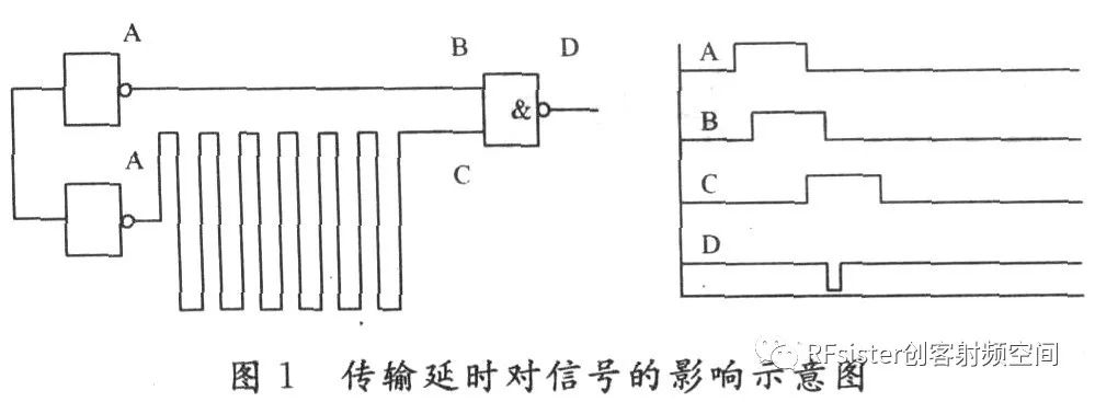
Delay refers to that the signal is transmitted at a limited speed on the wire of the PCB board, and the signal is sent from the sending end to the receiving end with a transmission delay therebetween. The delay of the signal will influence the timing of the system, and the transmission delay mainly depends on the length of the wire and the dielectric constant of the medium around the wire. In a high-speed digital system, the length of the signal transmission line is the most direct factor influencing the phase difference of the clock pulse. The phase difference of the clock pulse refers to two clock signals generated at the same time, and the time to reach the receiving end is not synchronized. Clock phase difference reduces the predictability of arrival of the signal edge. If the clock phase difference is too large, an erroneous signal will be generated at the receiving end. As shown in FIG. 1, the transmission line delay has become an important part of the clock pulse period.
2.2 Reflection
Reflection is an echo on a subtransmission line. When the signal delay time (Delay) is much greater than the transition time (Transition Time), the signal line must be treated as a transmission line. When the characteristic impedance of the transmission line does not match the load impedance, part of the signal power (voltage or current) is transmitted to the line and reaches the load, but part of it is reflected. If the load impedance is less than the original impedance, the reflection is negative; otherwise, the reflection is positive. Changes in the geometry of the wiring, improper wire termination, transmission through the connector, and discontinuity in the power plane can all cause such reflections.
2.3 Synchronous Switching Noise (SSN)
When many digital signals on the PCB are synchronously switched (such as the CPU's data bus, address bus, etc.), due to impedances on the power line and ground line, synchronous switching noise will occur, and ground plane rebound will also occur on the ground line. Noise (ground bounce). The strength of the SSN and ground bombs also depends on the I/O characteristics of the integrated circuit, the impedance of the PCB board power plane and plane layers, and the layout and routing of high-speed devices on the PCB board.
2.4 Crosstalk
Crosstalk is the coupling between two signal lines, and mutual inductance and mutual capacitance between signal lines cause noise on the line. Capacitive coupling induces a coupling current, while inductive coupling induces a coupling voltage. Crosstalk noise originates from the electromagnetic coupling between the signal line networks, between the signal system and the power distribution system, and between vias. Stringing may cause false clocks, intermittent data errors, and the like, which may affect the transmission quality of adjacent signals. In fact, we do not need to completely eliminate the string winding, as long as it is controlled within the range that the system can withstand. PCB board parameters, signal line spacing, the electrical characteristics of the driving and receiving ends, and the baseline termination mode all have a certain effect on crosstalk.
2.5 Overshoot and Undershoot
Overshoot means that the first peak or valley exceeds the set voltage. For the rising edge, it means the highest voltage, and for the falling edge it means the lowest voltage. Undershoot means that the next valley or peak exceeds the set voltage. Excessive overshoot can cause the protection diode to work, leading to its premature failure. Excessive undershoot can cause false clock or data errors (misoperations).
2.6 Ringing and Rounding
The oscillation phenomenon is repeated overshoot and undershoot. The oscillation of the signal, which is the oscillation caused by the inductance and capacitance of the transitions on the line, belongs to the under-damped state, and the surrounding oscillation is an over-damped state. Oscillation and oscillating oscillations are caused by many factors as well as reflections. Oscillation can be reduced by proper termination, but it cannot be completely eliminated.
2.7 ground level rebound noise and return noise
When there is a large current surge in the circuit, it will cause ground plane rebound noise. If a large number of chip outputs are turned on at the same time, there will be a large transient current flow through the power plane of the chip and the board, the chip package and the power supply. Plane inductors and resistors can cause power supply noise. This can cause voltage fluctuations and changes in the true ground plane (OV). This noise can affect the operation of other components. The increase of the load capacitance, the decrease of the load resistance, the increase of the ground inductance, and the increase of the number of the switching devices all result in an increase in ground bounce. Since the ground plane (including power and ground) is divided, for example, the ground is divided into digital ground, analog ground, shield ground, etc., the ground plane return noise is generated when the digital signal goes to the analog ground area. Similarly, the power plane may also be divided into 2.5 V, 3.3 V, 5 V, and so on. Therefore, in the multi-voltage PCB design, the bounce noise and return noise of the ground plane require special attention.
3. Signal integrity solution
The problem of signal integrity is not caused by a single factor, but is caused by a combination of factors in the board design. The main signal integrity problems include reflection, ringing, ground bounce, crosstalk, etc. The following mainly describes crosstalk and reflection. The solution.
3.1 Crosstalk Analysis
Crosstalk is when the signal travels on a transmission line, causing unwanted voltage noise interference to adjacent transmission lines due to electromagnetic coupling. Excessive crosstalk can cause false triggering of the circuit, causing the system to malfunction. Since the crosstalk size is inversely proportional to the line spacing, it is proportional to the parallel length of the line. Crosstalk varies with circuit load. For the same topology and wiring, the greater the load, the greater the crosstalk. Crosstalk is proportional to the signal frequency. In a digital circuit, the edge change of the signal has the greatest effect on crosstalk. The faster the edge change, the greater the crosstalk. For these characteristics of crosstalk, it can be summarized as the following methods to reduce crosstalk:
(1) When possible, reduce the conversion rate of the signal edge by selecting the slow device while satisfying the design specification at the time of device selection, and avoid mixing different types of signals because of the rapidly changing signal There is a potential risk of crosstalk to slow-transforming signals.
(2) Crosstalk caused by capacitive coupling and inductive coupling increases with the increase of the load impedance of the disturbed line, so reducing the load can reduce the influence of coupling interference.
(3) If the wiring conditions permit, minimize the parallel length between adjacent transmission lines or increase the distance between capacitive coupling wires. For example, if the 3W principle is adopted (the spacing between the wires must be a single wire. The width of 3 times or the distance between two traces must be more than 2 times the width of a single trace. It is more effective to isolate the ground between the wires.
(4) Inserting a ground line between adjacent signal lines can also effectively reduce capacitive crosstalk. This ground line needs to be connected to the ground every 1/4 wavelength.
(5) Inductive coupling is more difficult to suppress. The number of loops should be reduced as much as possible, and the loop area should be reduced. The signal loops should avoid sharing the same wire.
(6) The signal layer traces of two adjacent layers should be vertical. Try to avoid parallel traces and reduce crosstalk between layers.
(7) There is only one reference plane in the surface layer, and the coupling of the surface wiring is stronger than that of the middle layer. Therefore, signals sensitive to crosstalk should be placed on the inner layer as much as possible.
(8) Through termination, the far end and near end of the transmission line and termination impedance match the transmission line, which can greatly reduce crosstalk and reflection interference.
3.2 Reflection Analysis
When a signal propagates on a transmission line, reflection occurs as soon as an impedance change is encountered. The main method for solving the reflection problem is to perform termination impedance matching.
3.2.1 Typical Termination Strategy for Transmission Lines In high-speed digital systems, impedance mismatches on transmission lines can cause signal reflection. The method of reducing and eliminating reflections is based on the characteristic impedance of the transmission line to perform termination impedance matching at its transmitting or receiving end. Let the source reflection coefficient or load reflection coefficient be O. The length of the transmission line meets the following conditions: Termination technology should be used: L>tr/2tpd. In the formula, L is the transmission line length; tr is the signal rise time of the source end; tpd is the load transmission delay per unit length on the transmission line. Termination of the transmission line usually uses two strategies: matching the impedance of the load with the impedance of the transmission line, ie parallel termination; matching the source impedance with the transmission line impedance, ie serial termination.
(1) Parallel termination Parallel termination is mainly to connect the pull-up or pull-down impedance as close to the load end as possible to achieve the impedance matching of the terminal. According to different application environments, the parallel termination can be further divided as shown in Figure 2. Several types.
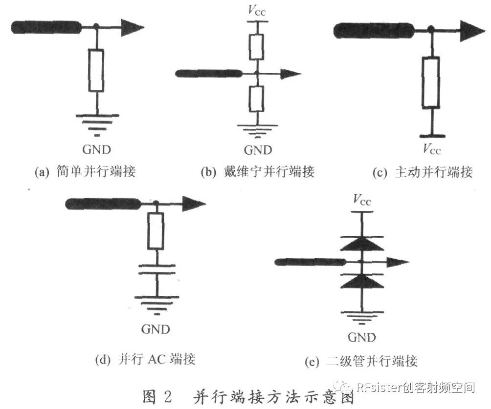
(2) Serial termination Serial termination is achieved by serially inserting a resistor into the transmission line as close to the source as possible. The serial termination is the impedance of the matching signal source, and the resistance of the inserted serial resistor is added. The output impedance of the upper drive source should be greater than or equal to the transmission line impedance. This strategy reduces the reflection coefficient at the source to zero, thereby suppressing the signal reflected from the load (the input is high impedance at the load and does not absorb energy) and is reflected back from the source to the load.
3.2.2 Termination Technology for Different Process Devices
The impedance matching and termination scheme will vary with the length of the interconnect and the logic device family in the circuit. Only the correct and appropriate termination method can effectively reduce the signal reflection for the specific situation. In general, for a driving source of a CMOS process, the output impedance value is relatively stable and close to the impedance value of the transmission line, so that the use of a serial termination technology for a CMOS device will achieve better results; and the driving source of the TTL process is The output impedance is different when the output logic is high and low. At this time, it is a better strategy to use the parallel Thevenin termination scheme; ECL devices generally have very low output impedance, and therefore receive at the ECL circuit. The use of a pull-down termination resistor to absorb energy is a universal termination technique for ECL circuits. Of course, the above method is not absolute either. Specific circuit differences, network topology selection, and the number of loads at the receiving end are all factors that can affect the termination strategy. Therefore, when implementing a circuit termination scheme in a high-speed circuit, it is necessary to Conditions to select the appropriate termination scheme to obtain the best termination effect.
4. Signal integrity analysis modeling
Proper circuit modeling and simulation are the most common solutions for signal integrity. In high-speed circuit design, simulation analysis shows more and more advantages. It gives designers accurate, intuitive design results that facilitate early detection and timely modification, thereby reducing design time and design costs. There are three commonly used: SPICE model, IBIS model, Verilog-A model. SPICE is a powerful general-purpose analog circuit simulator. It consists of two parts: Model Equation and Model Parameters. Thanks to the model equations, the SPICE model and the simulator's algorithm can be very closely linked to obtain better analysis efficiency and analysis results. The IBIS model is dedicated to digital signal integrity at the PCB level and system level. Analytical model. It describes the characteristics of digital integrated circuit I/O units and pins in the form of I/V and V/T tables. The analysis accuracy of the IBIS model mainly depends on the data points and data accuracy of the 1/V and V/T tables. Degree, compared with SPICE model, IBIS model calculation is very small.
5. Simulation verification
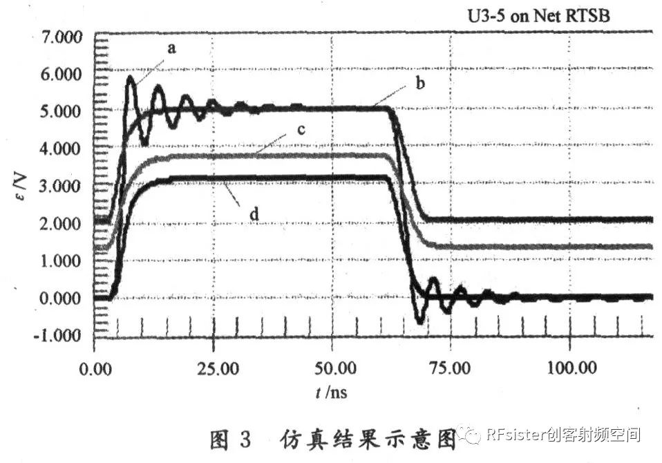
Asynchronous transponder example circuits are used to present the results. In the simulation environment, the excitation signal is set to 50 ns, the power supply is set to 5 V, and other settings are set by default. The simulation is performed on the U3-5 pin of the RTSB network. The simulation results are shown in Figure 3: a curve is the signal waveform before termination. See that there is a serious signal reflection; curve b, c is the signal waveform after the ground termination resistance, termination resistance value is different; d curve is the signal waveform after David South termination, it can be seen from the figure that the termination resistance can be Basically eliminate the reflection, the disadvantage is that the termination resistor to ground to a high level voltage drop, the termination resistor to the power supply makes the power supply low level.
6. Conclusion
With the continuous development of microelectronics technology, the use of high-speed devices and the design of high-speed digital systems are increasing. The system data rate, clock rate, and circuit density are all increasing, and the design requirements for PCBs are also increasing. It is a signal integrity problem. To ensure that the PCB has a good signal integrity, we must integrate a variety of factors, rational layout, wiring, and thus improve product performance.
The Smart Screen Protector Cutting Machine can help stores reduce the inventory of Screen Protectors. It is mainly used to cut Screen Protectors such as Mobile Phone Screen Protectors, Watch Screen Protectors, Tablet Screen Protectors, Pad Screen Protectors, and personalized fashion Back Films. It is very suitable for personal business or shop drainage.
Universal Screen Protector Cutting Machine has 20000+ cloud data of different specifications and models, adopts massive cloud database, and all data is updated synchronously in the state of networking. You'll have a full range of screen protector models on one machine and cut any Screen Protector model as needed without having to stock up on Screen Protectors for various phone models. No more losing customers due to missing models.
Screen Protector Cutting Machine,Protective Film Cutting Machine,Back Sticker Cutting Machine,Phone Sticker Cutting Machine, Film Cutting Machine
Shenzhen Jianjiantong Technology Co., Ltd. , https://www.tpuprotector.com