In multi-channel multiplexed data acquisition systems, increasing the number of channels per ADC can improve the overall cost, area, and efficiency of the system. Modern SAR ADCs have high throughput and energy efficiency, allowing system designers to achieve higher channel densities than ever before.
Today we will show that settling transients at the input of the multiplexer (caused by large-scale switching transients at the output of the multiplexer) result in longer acquisition times and a significant reduction in the overall throughput of the multi-channel data acquisition system. The article will then focus on the design trade-offs needed to minimize input setup time and improve data throughput and system efficiency.
What is a multi-channel DAQ?
How to measure the performance of multi-channel DAQ?
A multi-channel data acquisition (DAQ) system is a complete signal chain subsystem that interfaces with multiple inputs (usually sensors). Its main function is to convert the analog signals at the input to digital data that the processing unit can understand. The main components of a multi-channel DAQ system are analog front-end subsystems (buffers, switching elements, and signal conditioning modules), ADCs, and digital interfaces. For high-speed precision converters, switching elements (usually multiplexers) are placed in front of the ADC driver and the converter itself to take advantage of the advanced features of modern ADCs. SAR ADCs combine high speed with high accuracy and are the most commonly used ADC types for these applications.
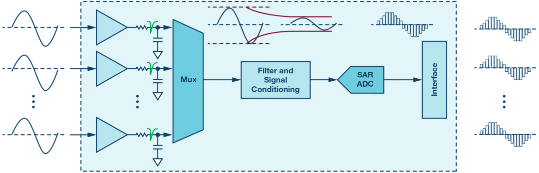
Figure 1. Block diagram of a typical SAR ADC-based multiplexed data acquisition system
High-channel-density precision DAQ systems for industrial and medical applications aim to compress the most channels into the smallest possible area. Multiplexed DAQ systems can generally achieve high density, high throughput, and good energy efficiency by:
Using High-Speed ​​Precision SAR ADCs
Use the lowest sampling rate for each channel
Maximize SAR ADC Converter Utilization
among them:
 |
n is the number of channels. For each converter, the total throughput of the multi-channel data acquisition system is given by:
 |
This shows that the total throughput of a multi-channel DAQ system depends not only on the speed and resolution of the SAR ADC, but also on the utilization of this converter.
How does latency affect the performance of multi-channel DAQ systems?In the case of a setup delay, the actual sampling and conversion period of the ADC will increase by one td, resulting in the actual maximum sampling rate of the converter given by:
 |
Where TADC is the sampling period for each sample of the ADC (most ADC data sheets are usually provided, the more common form is the reciprocal of the SAR ADC sampling rate, in "seconds/sample"). For non-zero delay td, the actual maximum sampling rate of a multi-channel DAQ system is always less than the converter sampling rate, resulting in converter utilization consistently below 100%. It can be seen from this that any increase in the sampling and conversion cycles will reduce the converter's utilization. When associated with the previous expression on total throughput, the maximum number of channels that a multi-channel DAQ can accommodate is reduced. In short, any setup delay will reduce the channel density and/or total throughput of multi-channel DAQ systems.
What is a multiplexer input switching glitch and input setup time?When the multiplexer switches from one input to the other input, the output still has the memory of the previous input channel in the form of the charge stored in the multiplexer's output load capacitance and parasitic drain capacitance. This is more noticeable for high capacitive loads (such as the ADC driver and the ADC itself) because these stored charges do not have low impedance paths to go. It can even be said that these charges are trapped because the output is capacitive, and modern multiplexers use a break-before-make (BBM) mechanism, so the multiplexer has a high impedance. Only by switching to the next input can these charges be discharged.
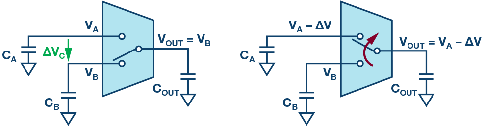
Figure 2. Pre-switching state (left), after switchover, charge sharing occurs, quickly causing voltage drop ΔV (right)
After switching, the input capacitor CA will be connected in parallel to the output capacitor COUT. However, CA and COUT may initially be at different potentials, which will lead to charge sharing between CA and COUT. For ultra-high bandwidth multiplexers, charge sharing occurs almost instantaneously, causing high frequency glitches at the multiplexer input. The amplitude ΔV of this glitch is given by:
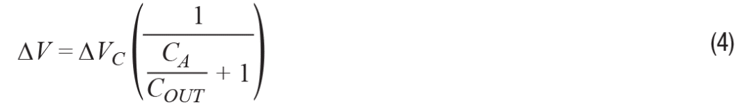 |
Where ΔVC is the difference in capacitor voltage before switching. Transient glitches on the input side of the multiplexer are known as kickbacks and are more common for switching applications with high capacitive loads such as ADCs, capacitive DACs, and sampling circuits. For the converter to generate valid data, the glitch must settle within 1 LSB of the output, and the time required for the input to settle within 1 LSB (and stay within this range!) is the input setup time (tS). tS is part of the delay td described earlier, and its contribution to this term is probably the largest.
When the ADC is not as fast as it is now, these glitches and the corresponding input setup time are negligible and negligible. However, as the ADC speed increases, the converter sampling period becomes shorter and shorter, close to the input settling time. As mentioned earlier, when the ADC period TADC equals the input setup time tS (actually td), the converter utilization is greatly reduced to 50%. This means we only use half the capacity of the converter! The importance of input setup time needs to be reiterated. It should be synchronized with the current technology of precision converters to pave the way for improving the performance of multi-channel DAQ systems.
How to minimize input setup time?To minimize switching glitches, an RC filter is usually used between the buffer amplifier and the multiplexer, called the buffer network. Figure 3 shows the signal chain subsystem and its corresponding switching timing diagram for a dual-channel multiplexed analog front-end subsystem.

Figure 3. Dual-channel multiplexed analog front-end subsystem and corresponding timing diagram for a multi-channel DAQ system
With buffer RC as the dominant pole, input glitches and settling transients can be approximated as having a first-order (exponential) response, assuming that the multiplexer has a very high bandwidth relative to the amplifier and buffer RC. To further analyze the input glitch, Figure 4 details the input glitch transient response.
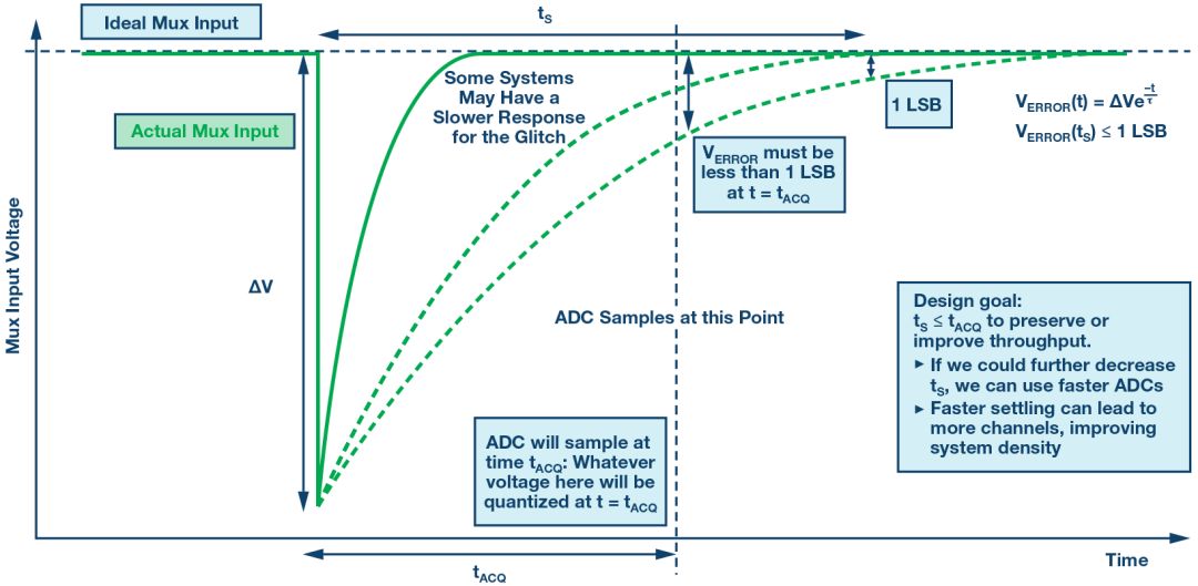
Figure 4. Multiplexer input glitch during analysis switchover: timing definition and design goals
For the first-order hypothesis, the expression of the error VERROR is a degressive exponential function with respect to time. The initial value of VERROR (the value at the time of switching) is the glitch amplitude ΔV, which will decay at the rate determined by the buffer RC value. The time it takes for VERROR to settle within 1 LSB is defined as the input setup time.
On the other hand, the converter samples at a period of tACQ (also called acquisition time). During the ADC conversion phase after the tACQ has elapsed, the converter quantizes any available sampling data. If VERROR decays too slowly, causing it not to settle within a certain value (1 LSB to several LSBs), problems can arise. This will cause the current sample to be corrupted by the previous analog input, causing crosstalk between the ADC channels. Considering the input setup time, it must be ensured that the input setup time is less than the converter acquisition time to minimize the error. Moreover, further reductions in tS also provide opportunities for using faster converters to increase overall system throughput and density.
Using our mathematical skills, the worst-case fastest input settling time expression can be derived when ΔVC is the full-scale input range and VERROR reaches at least 1 LSB (the multiplexer output is within 1 LSB of the target level). . Multi-channel DAQ system designers will have two design handles: the buffer time constant and the CA/COUT ratio to derive the expression of the input setup time:
 |
It can be seen here that the input settling time is a linear function of the number of time constants η required for the buffer time constant τ and VERROR to settle within 1 LSB. The most straightforward way to reduce the input setup time is to use a buffer network with a small time constant, which makes sense because the faster (high bandwidth) buffer network reduces the time constant. However, this approach will bring a different set of tradeoffs related to noise and load. On the other hand, minimizing the η term can also achieve similar results.
η is a function of the ratio of buffer capacitance (CA) to output capacitance (COUT). If 1 LSB is equal to the full-scale input range divided by 2 to the N-1 power (N is the number of bits), and the worst-case ΔVC is equal to the full-scale input range, the expression can be further simplified.
 |
Equation 6 may not be so intuitive and difficult to visualize, so using only semi-logarithmic plots of 10-bit, 14-bit, 18-bit, and 20-bit resolution might be better, as shown in Figure 5.

Figure 5. Graph to establish the time constant required to 1 LSB
It can be seen that the higher the CA/COUT value, the shorter the settling time; when the capacitance ratio is very high, the settling time is even close to zero. COUT is essentially the drain capacitance of the multiplexer and the input capacitance at subsequent stages, so only the CA remains flexible. For 10-bit resolution, the CA must be at least 1000 times larger than COUT for a settling time of 0, and at least 1,000,000 times larger than COUT for a 20-bit system! For example, for 10-bit and 20-bit systems, for a settling time of 0, a typical load of 100 pF requires 100 nF and 100 μF of buffer capacitance, respectively.
In short, minimizing the input setup time can be achieved in two ways:
Use high bandwidth for buffer networks;
Use a higher CA value than COUT.
High bandwidth and large buffer capacitance minimize input setup time, so use the highest bandwidth and maximum capacitance on the line?Not! The RC load effect and the amplifier's drive capability must be considered! In order to study the buffer network impact on the buffer amplifier, the analog front-end subsystem should be analyzed in the frequency domain.
Since we have input glitches built on the idea of ​​first-order response, the buffer network pole should be the main contributor. In other words, the buffer bandwidth should be smaller than the bandwidth of the buffer amplifier and multiplexer to avoid multipole interactions and to ensure that the first order approximation holds.
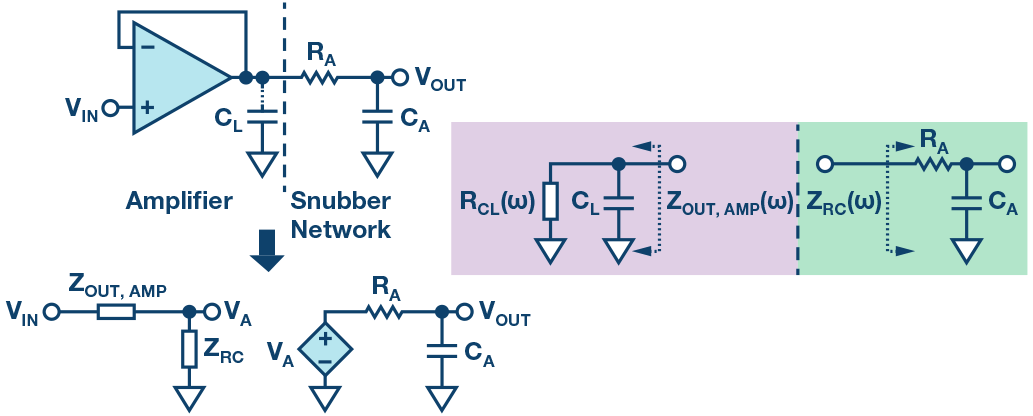
Figure 6. Equivalent impedance of buffer and buffer equivalent circuit (left) and amplifier and buffer network (right)
A typical buffer architecture consists of a buffered (G = 1) configured cascade of precision amplifiers and buffer networks. Analyzed in the frequency domain, the output of this subsystem depends on the ratio of the buffer input impedance to the sum of the buffer input impedance and the amplifier closed-loop output impedance. Examination shows that in order to avoid load effects, the buffer input impedance should be greater than the amplifier closed-loop impedance, as shown in Equation 7.
 |
That is, in order to avoid the buffer network becoming the load of the buffer amplifier, we should:
Increase buffer time constant RACA to effectively reduce bandwidth
Use a smaller buffer capacitor CA
Choose an amplifier with a very low closed-loop output impedance
The first two options allow us to clearly understand the trade-off between load effects and input setup time. This limits the buffer bandwidth and capacitance that we can use. The third option introduces a performance parameter that should be considered when selecting the appropriate precision amplifier. Also consider stability and driveability.
Figure 7 shows that for a precision amplifier with sufficient bandwidth (for example, an ADA4096-2 with a -3 dB closed loop bandwidth of approximately 970 kHz, the results are consistent with the current analysis, with the exception of a few waveforms. For a buffer bandwidth of 10 kHz, the maximum CA The fastest input settling time occurs, while for a buffer bandwidth of 200 kHz, increasing the CA still accelerates the settling time until a loading effect occurs. The underdamped response seen from the results has a very small glitch amplitude, but the settling time The response from a smaller CA is longer, despite the higher glitches in the latter, which highlights the importance of carefully studying how the buffer loads the amplifier and must be considered when selecting a device for the system.

Figure 7. ADA4096-2 Amplifier Model for Multiplexer Inputs for 10 kHz (Upper) and 200 kHz (Lower) Buffer Bandwidths
As mentioned earlier, one of the amplifier parameters that needs attention is the closed-loop output impedance. The closed loop impedance of an op amp is usually inversely proportional to its open loop gain, AV. We also want the buffer network to have a high bandwidth to minimize the settling time, thus requiring the -3 dB bandwidth of the amplifier to be even larger than the buffer bandwidth. In addition to lower noise, offset and offset drift, precision amplifiers best suited for multiplexed DAQ systems to achieve minimum input settling time have two priority features: 1) high bandwidth, 2) very low Closed loop impedance. However, these advantages are not without cost, and the cost is expressed in terms of power consumption. For example, we can look at the closed-loop impedance of the ADA4096-2 and ADA4522-2 shown in Figure 8.
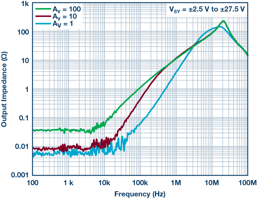
Figure 8a. Closed-loop impedance diagram in the ADA4522-2 data sheet

Figure 8b. Closed-loop impedance diagram in the ADA4096-2 data sheet
Considering the closed-loop output impedance diagram in the data sheet, and the ADA4522-2's -3 dB closed-loop bandwidth of 6 MHz (nominal), it is clear that it is a more suitable driver for this application. However, when power consumption is a priority, the ADA4096-2 has a supply current of 60 μA (typical) per amplifier and is more attractive than the ADA4522-2's 830 μA (typ) per amplifier. Despite this, both precision amplifiers can be used, depending on what the application really needs to achieve.
How do we do the best?In order to maximize the density and throughput of multi-channel DAQ systems, the input setup time should be less than or equal to the ADC acquisition time, any additional delay will reduce the performance of multi-channel DAQ systems;
To minimize the input setup time, the bandwidth and capacitance of the buffer network need to be increased, but care must be taken when selecting component values ​​to avoid load effects in the frequency domain.
Choosing the most suitable precision amplifier requires trade-offs in power consumption, closed-loop output impedance, and -3 dB bandwidth, which are prioritized according to the real needs of the application.
Flexible Cables
Application: Those electric wires are suitable for internal wiring or supply cords to electrical apparatus.
- IEC60227, BS 6004
- 300/500V 450/750V
- Certification: CE
- Flame retardant or fire resistance or Low smoking and Halogen free or other property can be available
Flexible Cables,Outdoor Flex Cable,Rubber Cable,Flexible Cable Wire
Shenzhen Bendakang Cables Holding Co., Ltd , https://www.bdkcables.com