The Blackfin processor is the first 4th generation DSP product based on the Micro Signal Architecture (MSA) jointly developed by Analog Devices (ADI) and Intel Corporation. It is a large series of 16-bit products from Analog Devices. The ADSP-BF533 used in this article is a typical representative of the Blackfin series of processors.
The communication between the SPORTS port and the CH376 is realized by the SPI interface protocol. A communication design scheme based on USB master-slave interface chip CH376 and Blackfin533 is described, including the interface configuration of the SPORTs port, the hardware design of the USB module, the driver, and the driver of the CH376 chip. The DSP realizes the read/write access to the USB storage device and the communication between the computer and the DSP. Experiments show that the whole design can realize fast reading and writing of the U disk and facilitate communication with the PC.
1 Design principle
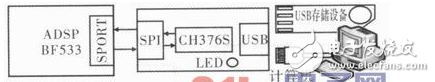
The module mainly realizes the communication between DSP and computer and the storage of data. The DSP-based USB master-slave bidirectional communication design scheme, through the ADSP BF533 SPORTs analog SPI port, completes the communication between ADSP and CH376, realizes the two-way communication between DSP and PC, DSP and U disk, and freely switches between the two modes. The overall block diagram of the system.
2 chip introduction
2.1 CH376 chip
CH376 is a file management control chip produced by Nanjing Yuheng Company. CH376 supports USB device mode and USB host mode, and has built-in basic firmware of USB communication protocol, dedicated communication protocol firmware for processing Mass-Storage mass storage device, communication interface firmware of SD card, FAT16 and FAT32, and management firmware of FAT12 file system. Supports commonly used USB storage devices and SD cards.
CH376 supports 3 communication interfaces: 8-bit parallel port, SPI interface or asynchronous serial port. The controller such as the MCU/DSP/MCU/MPU can control the CH376 chip through the above communication interface, access the files in the U disk and the SD card or communicate with the computer.
2.2 ADSP-BF533 chip
The ADSP-BF533 processor is one of the Blackfin family of products and is a new 16-bit embedded processor designed to meet the computational requirements and low power requirements of embedded audio, video and communications applications. Based on the MicroSignal Architecture (MSA) jointly developed by ADI and Intel, it combines a 32-bit RISC instruction set and dual 16-bit multiply-accumulate (MAC) signal processing with the ease of use of a general-purpose microcontroller. Sexual combination. The ADSP-BF533 processor has a wealth of peripheral resources, including a UART port, an SPI port, two serial ports (SPORTs), and a PF port.
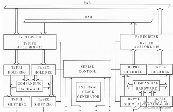
The Blackfin533 has two identical synchronous serial ports, SPORT0 and SPORT1. These two serial ports support a variety of serial data communication protocols. Figure 2 is a simplified block diagram of the SPORT. The data to be transmitted is written from the internal register to the memory map register SPORTx_TX of SPORT. Depending on the selection, this data can be automatically transferred to the shift register by hardware or not, or hardware companding. The shift register bits are shifted out of the DT pin of the SPORT, with the most significant or least significant bit being in front and synchronized with the clock on the TCLK pin. The receiving portion of the SPORT receives data from the DR and synchronizes with the serial clock. After receiving a complete word, the data is automatically transferred to the SPORT's memory-mapped register SPORTx_TX, which is accessible by the processor.
3 hardware design
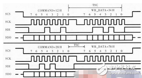
CH376 always inputs data from the rising edge of SPI clock SCK, while the output is allowed to output data from the falling edge of SCK. The data bit order is high first, and 8 bits are 1 byte. The DSP issues 1 Byte data according to the SPI output mode. The first byte received by CH376 after the SPI chip selects the SCS is regarded as the command code, and the subsequent byte is regarded as the data. During the write operation, the DSP issues 1 Byte of data to be written to CH376. After waiting for the SPI interface to be idle, the DSP continues to issue a number of bytes of data to be written. CH376 accepts in turn until the DSP disables the SPI chip select; when the read operation, the DSP CH376 receives 1 Byte of data. After waiting for the SPI interface to be idle, the DSP continues to receive several bytes of data from CH376 until the DSP disables SPI chip select. Figure 3 is a logic timing diagram of the SPI interface. The previous one issues the command 12H and writes the data 34H, the latter one issues the command 28H and reads the data 78H.
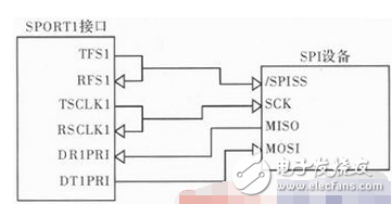
In order to realize the USB master-slave two-way communication design scheme of DSP, the DSP's SPORTs interface is simulated with the SPI interface and communicates with the device supporting the SPI interface communication mode. The SPI interface in master mode requires four signals: data input (MISO), data output (MOSI), clock (SCK), and chip select (/SPISS). Three of these four signals correspond to the SPORTs interface: (1) MOSI corresponds to the transmission pin (DTxPRI) of the SPORTS port. (2) MISO corresponds to the acceptance pin (DRxPRI) of the SPORTS port. (3) SCK corresponds to the clock pin (TSCLKx/RSCLKx) of the SPORTS port.
The pin signal in the SPI interface that does not correspond to the SPORTs interface is the chip select signal. The chip select signal (/SPISS) is used as a strobe for the clock SCK in the SPI interface. As an SPI slave, only the chip select/SPISS is pulled low and the response occurs on the edge of the clock signal SCK. Once the device is enabled for communication, the SPORTs master will generate a continuous clock. To emulate the SPORTs port with the SPI port, the correct timing and chip select/SPISS signals are the focus. When TFS is configured low, data is placed on the transmit pin DTxPRI of the SPORTs during the same period, and the TFS signal is always pulled low during data transmission until the new data starts to be transmitted, which happens to be with the SPI interface/ The SPISS signal is consistent. On the contrary, as the slave mode, the same is true. Therefore, the synchronous timing signal simulation / SPISS chip select signal of the SPORTS interface can meet the requirements. The hardware connection is shown in Figure 4.
The system hardware circuit is shown in Figure 5. The system configures CH376 as serial communication mode, using SPORT1 port. In DSP main mode, the data flow passes through the SPORT1 port of Blackfin533, and the SPI communication mode and CH376 module SPI port are simulated by the above configuration. Communication, when passing the external USB port, CH376 accesses the USB flash drive by USB-HOST. Conversely, when the DSP slave mode, the PC communicates with the Blackfin533 via USB port and CH376 by USB-SLAVE.
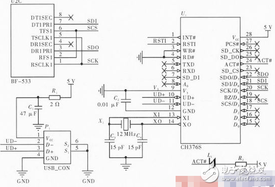
The SCS pin of the CH376 chip is driven by the DSP's SPORT port frame synchronization pins TFS and RFS. The SCK is sent by the DSP SPORT to transmit and receive the clock output pins TSCLK and RSCLK. The SDI pin is driven by the DSP SPORT data output pin DTxPRI. The SDO pin is connected to the SPORT data input pin DRxPRI of the DSP.
CH376 chip configuration, capacitor C2 is used for internal power supply node decoupling to reduce EMI during USB transmission. Crystal X1 is an oscillating circuit for providing system clock signal to CH376, P1 is USB port, and resistor R1 is used to limit output to The current of the external USB device, C1 is mainly used to reduce the power supply voltage ripple when the USB device is just inserted. Refer to the ADI official design manual for the peripheral circuit configuration of the Blackfin533.
4 software design
The CH376S reads and writes to the U disk into two types: sector mode and byte mode. The sector mode reads and writes U disk files in units of sectors. The read and write speed is fast, but usually requires an extra buffer. Byte mode reads and writes U disk files in units of bytes. The read/write speed is slow. It is usually used for reading and writing small data volumes, but it is convenient to use.
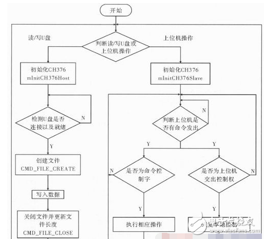
The system software flow is shown in Figure 6. The DSP determines that the user chooses to write the U disk operation or the host computer operation. When the U disk operation is selected, the CH376 chip is first initialized, and the U disk is continuously detected by the loop. When the U disk is ready, the file name is created, the data is written to the file, and the file is closed, and the file is started. When selecting the upper computer operation, connect the system to the PC through the USB data cable, first initialize the CH376 chip, and the DSP determines whether the upper computer software issues an operation command. If the command control word is issued, the corresponding operation is performed, and the judgment is continued. Whether the host computer issues a command word; if the command issued is the surrender control, the system resumes local control and enters the beginning.
5 experimental test
The test of the whole system design is mainly divided into U disk test and PC test.
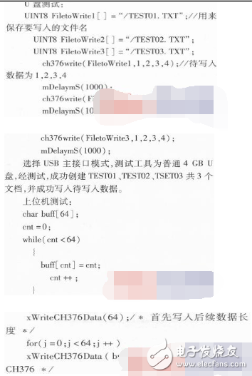
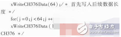
Select USB slave interface mode, the test tool is USB device CH372 or CH375 debugging tool. Since #define uREAD_DATA 0x80 is defined in the host computer program, in the debugging tool, set the port to transmit data as the receive data command 80. The experimental results show that 0~3F is successfully received in the endpoint upload, a total of 64 data. The experimental results are shown in Figure 7.
6 Conclusion
The design of USB master-slave interface based on ADSP-Blackfin533 SPORTs port is discussed in detail from hardware and software. It has the advantages of fast transmission speed, simple structure, convenient operation and large amount of data transmission. After testing, the performance is stable and reliable, and can be widely used in various practical occasions.
SHENZHEN CHONDEKUAI TECHNOLOGY CO.LTD , https://www.szfourinone.com